Verilog modules
PSoC Creator automatically generate a verilog file of your schematic design. This verilog file (PROJ_NAME.v) is under codegentemp directory located on your project directory.
Here's the verilog from a empty project using the CY8CKIT-059 PSoC 5LP kit:
// ======================================================================
// Design01.v generated from TopDesign.cysch
// 01/11/2017 at 16:34
// This file is auto generated. ANY EDITS YOU MAKE MAY BE LOST WHEN THIS FILE IS REGENERATED!!!
// ======================================================================
/* -- WARNING: The following section of defines are deprecated and will be removed in a future release -- */
`define CYDEV_CHIP_DIE_LEOPARD 1
`define CYDEV_CHIP_REV_LEOPARD_PRODUCTION 3
`define CYDEV_CHIP_REV_LEOPARD_ES3 3
`define CYDEV_CHIP_REV_LEOPARD_ES2 1
`define CYDEV_CHIP_REV_LEOPARD_ES1 0
`define CYDEV_CHIP_DIE_TMA4 2
`define CYDEV_CHIP_REV_TMA4_PRODUCTION 17
`define CYDEV_CHIP_REV_TMA4_ES 17
`define CYDEV_CHIP_REV_TMA4_ES2 33
`define CYDEV_CHIP_DIE_PSOC4A 3
`define CYDEV_CHIP_REV_PSOC4A_PRODUCTION 17
`define CYDEV_CHIP_REV_PSOC4A_ES0 17
`define CYDEV_CHIP_DIE_PSOC5LP 4
`define CYDEV_CHIP_REV_PSOC5LP_PRODUCTION 0
`define CYDEV_CHIP_REV_PSOC5LP_ES0 0
`define CYDEV_CHIP_DIE_PSOC5TM 5
`define CYDEV_CHIP_REV_PSOC5TM_PRODUCTION 1
`define CYDEV_CHIP_REV_PSOC5TM_ES1 1
`define CYDEV_CHIP_REV_PSOC5TM_ES0 0
`define CYDEV_CHIP_DIE_VOLANS 6
`define CYDEV_CHIP_REV_VOLANS_PRODUCTION 0
`define CYDEV_CHIP_DIE_BERRYPECKER 7
`define CYDEV_CHIP_REV_BERRYPECKER_PRODUCTION 0
`define CYDEV_CHIP_DIE_CRANE 8
`define CYDEV_CHIP_REV_CRANE_PRODUCTION 0
`define CYDEV_CHIP_DIE_FM3 9
`define CYDEV_CHIP_REV_FM3_PRODUCTION 0
`define CYDEV_CHIP_DIE_FM4 10
`define CYDEV_CHIP_REV_FM4_PRODUCTION 0
`define CYDEV_CHIP_DIE_EXPECT 4
`define CYDEV_CHIP_REV_EXPECT 0
`define CYDEV_CHIP_DIE_ACTUAL 4
/* -- WARNING: The previous section of defines are deprecated and will be removed in a future release -- */
`define CYDEV_CHIP_FAMILY_PSOC3 1
`define CYDEV_CHIP_FAMILY_PSOC4 2
`define CYDEV_CHIP_FAMILY_PSOC5 3
`define CYDEV_CHIP_FAMILY_FM0P 4
`define CYDEV_CHIP_FAMILY_FM3 5
`define CYDEV_CHIP_FAMILY_FM4 6
`define CYDEV_CHIP_FAMILY_UNKNOWN 0
`define CYDEV_CHIP_MEMBER_UNKNOWN 0
`define CYDEV_CHIP_MEMBER_3A 1
`define CYDEV_CHIP_REVISION_3A_PRODUCTION 3
`define CYDEV_CHIP_REVISION_3A_ES3 3
`define CYDEV_CHIP_REVISION_3A_ES2 1
`define CYDEV_CHIP_REVISION_3A_ES1 0
`define CYDEV_CHIP_MEMBER_4G 2
`define CYDEV_CHIP_REVISION_4G_PRODUCTION 17
`define CYDEV_CHIP_REVISION_4G_ES 17
`define CYDEV_CHIP_REVISION_4G_ES2 33
`define CYDEV_CHIP_MEMBER_4U 3
`define CYDEV_CHIP_REVISION_4U_PRODUCTION 0
`define CYDEV_CHIP_MEMBER_4E 4
`define CYDEV_CHIP_REVISION_4E_PRODUCTION 0
`define CYDEV_CHIP_MEMBER_4O 5
`define CYDEV_CHIP_REVISION_4O_PRODUCTION 0
`define CYDEV_CHIP_MEMBER_4N 6
`define CYDEV_CHIP_REVISION_4N_PRODUCTION 0
`define CYDEV_CHIP_MEMBER_4Q 7
`define CYDEV_CHIP_REVISION_4Q_PRODUCTION 0
`define CYDEV_CHIP_MEMBER_4D 8
`define CYDEV_CHIP_REVISION_4D_PRODUCTION 0
`define CYDEV_CHIP_MEMBER_4J 9
`define CYDEV_CHIP_REVISION_4J_PRODUCTION 0
`define CYDEV_CHIP_MEMBER_4K 10
`define CYDEV_CHIP_REVISION_4K_PRODUCTION 0
`define CYDEV_CHIP_MEMBER_4H 11
`define CYDEV_CHIP_REVISION_4H_PRODUCTION 0
`define CYDEV_CHIP_MEMBER_4A 12
`define CYDEV_CHIP_REVISION_4A_PRODUCTION 17
`define CYDEV_CHIP_REVISION_4A_ES0 17
`define CYDEV_CHIP_MEMBER_4F 13
`define CYDEV_CHIP_REVISION_4F_PRODUCTION 0
`define CYDEV_CHIP_REVISION_4F_PRODUCTION_256K 0
`define CYDEV_CHIP_REVISION_4F_PRODUCTION_256DMA 0
`define CYDEV_CHIP_MEMBER_4P 14
`define CYDEV_CHIP_REVISION_4P_PRODUCTION 0
`define CYDEV_CHIP_MEMBER_4M 15
`define CYDEV_CHIP_REVISION_4M_PRODUCTION 0
`define CYDEV_CHIP_MEMBER_4L 16
`define CYDEV_CHIP_REVISION_4L_PRODUCTION 0
`define CYDEV_CHIP_MEMBER_4I 17
`define CYDEV_CHIP_REVISION_4I_PRODUCTION 0
`define CYDEV_CHIP_MEMBER_4C 18
`define CYDEV_CHIP_REVISION_4C_PRODUCTION 0
`define CYDEV_CHIP_MEMBER_5B 19
`define CYDEV_CHIP_REVISION_5B_PRODUCTION 0
`define CYDEV_CHIP_REVISION_5B_ES0 0
`define CYDEV_CHIP_MEMBER_5A 20
`define CYDEV_CHIP_REVISION_5A_PRODUCTION 1
`define CYDEV_CHIP_REVISION_5A_ES1 1
`define CYDEV_CHIP_REVISION_5A_ES0 0
`define CYDEV_CHIP_MEMBER_PDL_FM0P_TYPE1 21
`define CYDEV_CHIP_REVISION_PDL_FM0P_TYPE1_PRODUCTION 0
`define CYDEV_CHIP_MEMBER_PDL_FM0P_TYPE2 22
`define CYDEV_CHIP_REVISION_PDL_FM0P_TYPE2_PRODUCTION 0
`define CYDEV_CHIP_MEMBER_PDL_FM0P_TYPE3 23
`define CYDEV_CHIP_REVISION_PDL_FM0P_TYPE3_PRODUCTION 0
`define CYDEV_CHIP_MEMBER_FM3 24
`define CYDEV_CHIP_REVISION_FM3_PRODUCTION 0
`define CYDEV_CHIP_MEMBER_FM4 25
`define CYDEV_CHIP_REVISION_FM4_PRODUCTION 0
`define CYDEV_CHIP_FAMILY_USED 3
`define CYDEV_CHIP_MEMBER_USED 19
`define CYDEV_CHIP_REVISION_USED 0
// top
module top ;
endmodule
 With the following configuration:


That Digital Output Pin with name LED generates:
wire [0:0] tmpOE__LED_net;
wire [0:0] tmpFB_0__LED_net;
wire [0:0] tmpIO_0__LED_net;
wire [0:0] tmpINTERRUPT_0__LED_net;
electrical [0:0] tmpSIOVREF__LED_net;
cy_psoc3_pins_v1_10
#(.id("e851a3b9-efb8-48be-bbb8-b303b216c393"),
.drive_mode(3'b110),
.ibuf_enabled(1'b1),
.init_dr_st(1'b0),
.input_clk_en(0),
.input_sync(1'b1),
.input_sync_mode(1'b0),
.intr_mode(2'b00),
.invert_in_clock(0),
.invert_in_clock_en(0),
.invert_in_reset(0),
.invert_out_clock(0),
.invert_out_clock_en(0),
.invert_out_reset(0),
.io_voltage(""),
.layout_mode("CONTIGUOUS"),
.oe_conn(1'b0),
.oe_reset(0),
.oe_sync(1'b0),
.output_clk_en(0),
.output_clock_mode(1'b0),
.output_conn(1'b0),
.output_mode(1'b0),
.output_reset(0),
.output_sync(1'b0),
.pa_in_clock(-1),
.pa_in_clock_en(-1),
.pa_in_reset(-1),
.pa_out_clock(-1),
.pa_out_clock_en(-1),
.pa_out_reset(-1),
.pin_aliases(""),
.pin_mode("O"),
.por_state(4),
.sio_group_cnt(0),
.sio_hyst(1'b1),
.sio_ibuf(""),
.sio_info(2'b00),
.sio_obuf(""),
.sio_refsel(""),
.sio_vtrip(""),
.sio_hifreq(""),
.sio_vohsel(""),
.slew_rate(1'b0),
.spanning(0),
.use_annotation(1'b0),
.vtrip(2'b10),
.width(1),
.ovt_hyst_trim(1'b0),
.ovt_needed(1'b0),
.ovt_slew_control(2'b00),
.input_buffer_sel(2'b00))
LED
(.oe(tmpOE__LED_net),
.y({1'b0}),
.fb({tmpFB_0__LED_net[0:0]}),
.io({tmpIO_0__LED_net[0:0]}),
.siovref(tmpSIOVREF__LED_net),
.interrupt({tmpINTERRUPT_0__LED_net[0:0]}),
.in_clock({1'b0}),
.in_clock_en({1'b1}),
.in_reset({1'b0}),
.out_clock({1'b0}),
.out_clock_en({1'b1}),
.out_reset({1'b0}));
assign tmpOE__LED_net = (`CYDEV_CHIP_MEMBER_USED == `CYDEV_CHIP_MEMBER_3A && `CYDEV_CHIP_REVISION_USED < `CYDEV_CHIP_REVISION_3A_ES3) ? ~{1'b1} : {1'b1};
 And the Control_Reg configuration (The DOP configuration is the same as b4)
 Resulting verilog file:
// Component: CyControlReg_v1_80
`ifdef CY_BLK_DIR
`undef CY_BLK_DIR
`endif
`ifdef WARP
`define CY_BLK_DIR "C:\Program Files (x86)\Cypress\PSoC Creator\4.0\PSoC Creator\psoc\content\cyprimitives\CyPrimitives.cylib\CyControlReg_v1_80"
`include "C:\Program Files (x86)\Cypress\PSoC Creator\4.0\PSoC Creator\psoc\content\cyprimitives\CyPrimitives.cylib\CyControlReg_v1_80\CyControlReg_v1_80.v"
`else
`define CY_BLK_DIR "C:\Program Files (x86)\Cypress\PSoC Creator\4.0\PSoC Creator\psoc\content\cyprimitives\CyPrimitives.cylib\CyControlReg_v1_80"
`include "C:\Program Files (x86)\Cypress\PSoC Creator\4.0\PSoC Creator\psoc\content\cyprimitives\CyPrimitives.cylib\CyControlReg_v1_80\CyControlReg_v1_80.v"
`endif
// top
module top ;
wire Net_10;
wire Net_9;
wire Net_8;
wire Net_7;
wire Net_6;
wire Net_5;
wire Net_4;
wire Net_3;
wire Net_2;
wire Net_1;
wire [0:0] tmpOE__LED_net;
wire [0:0] tmpFB_0__LED_net;
wire [0:0] tmpIO_0__LED_net;
wire [0:0] tmpINTERRUPT_0__LED_net;
electrical [0:0] tmpSIOVREF__LED_net;
cy_psoc3_pins_v1_10
#(.id("e851a3b9-efb8-48be-bbb8-b303b216c393"),
.drive_mode(3'b110),
.ibuf_enabled(1'b1),
.init_dr_st(1'b0),
.input_clk_en(0),
.input_sync(1'b1),
.input_sync_mode(1'b0),
.intr_mode(2'b00),
.invert_in_clock(0),
.invert_in_clock_en(0),
.invert_in_reset(0),
.invert_out_clock(0),
.invert_out_clock_en(0),
.invert_out_reset(0),
.io_voltage(""),
.layout_mode("CONTIGUOUS"),
.oe_conn(1'b0),
.oe_reset(0),
.oe_sync(1'b0),
.output_clk_en(0),
.output_clock_mode(1'b0),
.output_conn(1'b1),
.output_mode(1'b0),
.output_reset(0),
.output_sync(1'b0),
.pa_in_clock(-1),
.pa_in_clock_en(-1),
.pa_in_reset(-1),
.pa_out_clock(-1),
.pa_out_clock_en(-1),
.pa_out_reset(-1),
.pin_aliases(""),
.pin_mode("O"),
.por_state(4),
.sio_group_cnt(0),
.sio_hyst(1'b1),
.sio_ibuf(""),
.sio_info(2'b00),
.sio_obuf(""),
.sio_refsel(""),
.sio_vtrip(""),
.sio_hifreq(""),
.sio_vohsel(""),
.slew_rate(1'b0),
.spanning(0),
.use_annotation(1'b0),
.vtrip(2'b10),
.width(1),
.ovt_hyst_trim(1'b0),
.ovt_needed(1'b0),
.ovt_slew_control(2'b00),
.input_buffer_sel(2'b00))
LED
(.oe(tmpOE__LED_net),
.y({Net_1}),
.fb({tmpFB_0__LED_net[0:0]}),
.io({tmpIO_0__LED_net[0:0]}),
.siovref(tmpSIOVREF__LED_net),
.interrupt({tmpINTERRUPT_0__LED_net[0:0]}),
.in_clock({1'b0}),
.in_clock_en({1'b1}),
.in_reset({1'b0}),
.out_clock({1'b0}),
.out_clock_en({1'b1}),
.out_reset({1'b0}));
assign tmpOE__LED_net = (`CYDEV_CHIP_MEMBER_USED == `CYDEV_CHIP_MEMBER_3A && `CYDEV_CHIP_REVISION_USED < `CYDEV_CHIP_REVISION_3A_ES3) ? ~{1'b1} : {1'b1};
CyControlReg_v1_80 Control_Reg (
.control_1(Net_2),
.control_2(Net_3),
.control_3(Net_4),
.control_0(Net_1),
.control_4(Net_5),
.control_5(Net_6),
.control_6(Net_7),
.control_7(Net_8),
.clock(1'b0),
.reset(1'b0));
defparam Control_Reg.Bit0Mode = 0;
defparam Control_Reg.Bit1Mode = 0;
defparam Control_Reg.Bit2Mode = 0;
defparam Control_Reg.Bit3Mode = 0;
defparam Control_Reg.Bit4Mode = 0;
defparam Control_Reg.Bit5Mode = 0;
defparam Control_Reg.Bit6Mode = 0;
defparam Control_Reg.Bit7Mode = 0;
defparam Control_Reg.BitValue = 0;
defparam Control_Reg.BusDisplay = 0;
defparam Control_Reg.ExtrReset = 0;
defparam Control_Reg.NumOutputs = 1;
endmodule
 Here's the resulting verilog:
// ======================================================================
// PSoC4_Ctrl_Sts.v generated from TopDesign.cysch
// 01/14/2017 at 20:15
// This file is auto generated. ANY EDITS YOU MAKE MAY BE LOST WHEN THIS FILE IS REGENERATED!!!
// ======================================================================
`define CYDEV_CHIP_FAMILY_PSOC3 1
`define CYDEV_CHIP_FAMILY_PSOC4 2
`define CYDEV_CHIP_FAMILY_PSOC5 3
`define CYDEV_CHIP_FAMILY_FM0P 4
`define CYDEV_CHIP_FAMILY_FM3 5
`define CYDEV_CHIP_FAMILY_FM4 6
`define CYDEV_CHIP_FAMILY_UNKNOWN 0
`define CYDEV_CHIP_MEMBER_UNKNOWN 0
`define CYDEV_CHIP_MEMBER_3A 1
`define CYDEV_CHIP_REVISION_3A_PRODUCTION 3
`define CYDEV_CHIP_REVISION_3A_ES3 3
`define CYDEV_CHIP_REVISION_3A_ES2 1
`define CYDEV_CHIP_REVISION_3A_ES1 0
`define CYDEV_CHIP_MEMBER_4G 2
`define CYDEV_CHIP_REVISION_4G_PRODUCTION 17
`define CYDEV_CHIP_REVISION_4G_ES 17
`define CYDEV_CHIP_REVISION_4G_ES2 33
`define CYDEV_CHIP_MEMBER_4U 3
`define CYDEV_CHIP_REVISION_4U_PRODUCTION 0
`define CYDEV_CHIP_MEMBER_4E 4
`define CYDEV_CHIP_REVISION_4E_PRODUCTION 0
`define CYDEV_CHIP_MEMBER_4O 5
`define CYDEV_CHIP_REVISION_4O_PRODUCTION 0
`define CYDEV_CHIP_MEMBER_4N 6
`define CYDEV_CHIP_REVISION_4N_PRODUCTION 0
`define CYDEV_CHIP_MEMBER_4Q 7
`define CYDEV_CHIP_REVISION_4Q_PRODUCTION 0
`define CYDEV_CHIP_MEMBER_4D 8
`define CYDEV_CHIP_REVISION_4D_PRODUCTION 0
`define CYDEV_CHIP_MEMBER_4J 9
`define CYDEV_CHIP_REVISION_4J_PRODUCTION 0
`define CYDEV_CHIP_MEMBER_4K 10
`define CYDEV_CHIP_REVISION_4K_PRODUCTION 0
`define CYDEV_CHIP_MEMBER_4H 11
`define CYDEV_CHIP_REVISION_4H_PRODUCTION 0
`define CYDEV_CHIP_MEMBER_4A 12
`define CYDEV_CHIP_REVISION_4A_PRODUCTION 17
`define CYDEV_CHIP_REVISION_4A_ES0 17
`define CYDEV_CHIP_MEMBER_4F 13
`define CYDEV_CHIP_REVISION_4F_PRODUCTION 0
`define CYDEV_CHIP_REVISION_4F_PRODUCTION_256K 0
`define CYDEV_CHIP_REVISION_4F_PRODUCTION_256DMA 0
`define CYDEV_CHIP_MEMBER_4P 14
`define CYDEV_CHIP_REVISION_4P_PRODUCTION 0
`define CYDEV_CHIP_MEMBER_4M 15
`define CYDEV_CHIP_REVISION_4M_PRODUCTION 0
`define CYDEV_CHIP_MEMBER_4L 16
`define CYDEV_CHIP_REVISION_4L_PRODUCTION 0
`define CYDEV_CHIP_MEMBER_4I 17
`define CYDEV_CHIP_REVISION_4I_PRODUCTION 0
`define CYDEV_CHIP_MEMBER_4C 18
`define CYDEV_CHIP_REVISION_4C_PRODUCTION 0
`define CYDEV_CHIP_MEMBER_5B 19
`define CYDEV_CHIP_REVISION_5B_PRODUCTION 0
`define CYDEV_CHIP_REVISION_5B_ES0 0
`define CYDEV_CHIP_MEMBER_5A 20
`define CYDEV_CHIP_REVISION_5A_PRODUCTION 1
`define CYDEV_CHIP_REVISION_5A_ES1 1
`define CYDEV_CHIP_REVISION_5A_ES0 0
`define CYDEV_CHIP_MEMBER_PDL_FM0P_TYPE1 21
`define CYDEV_CHIP_REVISION_PDL_FM0P_TYPE1_PRODUCTION 0
`define CYDEV_CHIP_MEMBER_PDL_FM0P_TYPE2 22
`define CYDEV_CHIP_REVISION_PDL_FM0P_TYPE2_PRODUCTION 0
`define CYDEV_CHIP_MEMBER_PDL_FM0P_TYPE3 23
`define CYDEV_CHIP_REVISION_PDL_FM0P_TYPE3_PRODUCTION 0
`define CYDEV_CHIP_MEMBER_FM3 24
`define CYDEV_CHIP_REVISION_FM3_PRODUCTION 0
`define CYDEV_CHIP_MEMBER_FM4 25
`define CYDEV_CHIP_REVISION_FM4_PRODUCTION 0
`define CYDEV_CHIP_FAMILY_USED 2
`define CYDEV_CHIP_MEMBER_USED 12
`define CYDEV_CHIP_REVISION_USED 17
// Component: CyControlReg_v1_80
`ifdef CY_BLK_DIR
`undef CY_BLK_DIR
`endif
`ifdef WARP
`define CY_BLK_DIR "C:\Program Files (x86)\Cypress\PSoC Creator\4.0\PSoC Creator\psoc\content\cyprimitives\CyPrimitives.cylib\CyControlReg_v1_80"
`include "C:\Program Files (x86)\Cypress\PSoC Creator\4.0\PSoC Creator\psoc\content\cyprimitives\CyPrimitives.cylib\CyControlReg_v1_80\CyControlReg_v1_80.v"
`else
`define CY_BLK_DIR "C:\Program Files (x86)\Cypress\PSoC Creator\4.0\PSoC Creator\psoc\content\cyprimitives\CyPrimitives.cylib\CyControlReg_v1_80"
`include "C:\Program Files (x86)\Cypress\PSoC Creator\4.0\PSoC Creator\psoc\content\cyprimitives\CyPrimitives.cylib\CyControlReg_v1_80\CyControlReg_v1_80.v"
`endif
// Component: CyStatusReg_v1_90
`ifdef CY_BLK_DIR
`undef CY_BLK_DIR
`endif
`ifdef WARP
`define CY_BLK_DIR "C:\Program Files (x86)\Cypress\PSoC Creator\4.0\PSoC Creator\psoc\content\cyprimitives\CyPrimitives.cylib\CyStatusReg_v1_90"
`include "C:\Program Files (x86)\Cypress\PSoC Creator\4.0\PSoC Creator\psoc\content\cyprimitives\CyPrimitives.cylib\CyStatusReg_v1_90\CyStatusReg_v1_90.v"
`else
`define CY_BLK_DIR "C:\Program Files (x86)\Cypress\PSoC Creator\4.0\PSoC Creator\psoc\content\cyprimitives\CyPrimitives.cylib\CyStatusReg_v1_90"
`include "C:\Program Files (x86)\Cypress\PSoC Creator\4.0\PSoC Creator\psoc\content\cyprimitives\CyPrimitives.cylib\CyStatusReg_v1_90\CyStatusReg_v1_90.v"
`endif
// top
module top ;
wire Net_17;
wire [7:0] Net_13;
wire Net_12;
wire Net_10;
wire Net_9;
wire Net_11;
wire Net_8;
wire Net_7;
wire Net_6;
wire Net_5;
wire Net_3;
wire Net_2;
wire Net_1;
wire Net_4;
CyControlReg_v1_80 Control (
.control_1(Net_1),
.control_2(Net_2),
.control_3(Net_3),
.control_0(Net_4),
.control_4(Net_5),
.control_5(Net_6),
.control_6(Net_7),
.control_7(Net_8),
.clock(1'b0),
.reset(1'b0));
defparam Control.Bit0Mode = 0;
defparam Control.Bit1Mode = 0;
defparam Control.Bit2Mode = 0;
defparam Control.Bit3Mode = 0;
defparam Control.Bit4Mode = 0;
defparam Control.Bit5Mode = 0;
defparam Control.Bit6Mode = 0;
defparam Control.Bit7Mode = 0;
defparam Control.BitValue = 0;
defparam Control.BusDisplay = 0;
defparam Control.ExtrReset = 0;
defparam Control.NumOutputs = 8;
CyStatusReg_v1_90 Status (
.status_0(Net_4),
.status_1(Net_1),
.status_2(Net_2),
.status_3(Net_3),
.clock(Net_11),
.status_4(Net_5),
.status_5(Net_6),
.status_6(Net_7),
.status_7(Net_8),
.intr(Net_12),
.status_bus(8'b0));
defparam Status.Bit0Mode = 0;
defparam Status.Bit1Mode = 0;
defparam Status.Bit2Mode = 0;
defparam Status.Bit3Mode = 0;
defparam Status.Bit4Mode = 0;
defparam Status.Bit5Mode = 0;
defparam Status.Bit6Mode = 0;
defparam Status.Bit7Mode = 0;
defparam Status.BusDisplay = 0;
defparam Status.Interrupt = 0;
defparam Status.MaskValue = 0;
defparam Status.NumInputs = 8;
cy_clock_v1_0
#(.id("774c7934-bd75-45fc-a2b1-92f57c499c45"),
.source_clock_id(""),
.divisor(0),
.period("83333333.3333333"),
.is_direct(0),
.is_digital(0))
clk
(.clock_out(Net_11));
endmodule

Resulting verilog:
// ======================================================================
// XOR.v generated from TopDesign.cysch
// 01/15/2017 at 13:03
// This file is auto generated. ANY EDITS YOU MAKE MAY BE LOST WHEN THIS FILE IS REGENERATED!!!
// ======================================================================
`define CYDEV_CHIP_FAMILY_PSOC3 1
`define CYDEV_CHIP_FAMILY_PSOC4 2
`define CYDEV_CHIP_FAMILY_PSOC5 3
`define CYDEV_CHIP_FAMILY_FM0P 4
`define CYDEV_CHIP_FAMILY_FM3 5
`define CYDEV_CHIP_FAMILY_FM4 6
`define CYDEV_CHIP_FAMILY_UNKNOWN 0
`define CYDEV_CHIP_MEMBER_UNKNOWN 0
`define CYDEV_CHIP_MEMBER_3A 1
`define CYDEV_CHIP_REVISION_3A_PRODUCTION 3
`define CYDEV_CHIP_REVISION_3A_ES3 3
`define CYDEV_CHIP_REVISION_3A_ES2 1
`define CYDEV_CHIP_REVISION_3A_ES1 0
`define CYDEV_CHIP_MEMBER_4G 2
`define CYDEV_CHIP_REVISION_4G_PRODUCTION 17
`define CYDEV_CHIP_REVISION_4G_ES 17
`define CYDEV_CHIP_REVISION_4G_ES2 33
`define CYDEV_CHIP_MEMBER_4U 3
`define CYDEV_CHIP_REVISION_4U_PRODUCTION 0
`define CYDEV_CHIP_MEMBER_4E 4
`define CYDEV_CHIP_REVISION_4E_PRODUCTION 0
`define CYDEV_CHIP_MEMBER_4O 5
`define CYDEV_CHIP_REVISION_4O_PRODUCTION 0
`define CYDEV_CHIP_MEMBER_4N 6
`define CYDEV_CHIP_REVISION_4N_PRODUCTION 0
`define CYDEV_CHIP_MEMBER_4Q 7
`define CYDEV_CHIP_REVISION_4Q_PRODUCTION 0
`define CYDEV_CHIP_MEMBER_4D 8
`define CYDEV_CHIP_REVISION_4D_PRODUCTION 0
`define CYDEV_CHIP_MEMBER_4J 9
`define CYDEV_CHIP_REVISION_4J_PRODUCTION 0
`define CYDEV_CHIP_MEMBER_4K 10
`define CYDEV_CHIP_REVISION_4K_PRODUCTION 0
`define CYDEV_CHIP_MEMBER_4H 11
`define CYDEV_CHIP_REVISION_4H_PRODUCTION 0
`define CYDEV_CHIP_MEMBER_4A 12
`define CYDEV_CHIP_REVISION_4A_PRODUCTION 17
`define CYDEV_CHIP_REVISION_4A_ES0 17
`define CYDEV_CHIP_MEMBER_4F 13
`define CYDEV_CHIP_REVISION_4F_PRODUCTION 0
`define CYDEV_CHIP_REVISION_4F_PRODUCTION_256K 0
`define CYDEV_CHIP_REVISION_4F_PRODUCTION_256DMA 0
`define CYDEV_CHIP_MEMBER_4P 14
`define CYDEV_CHIP_REVISION_4P_PRODUCTION 0
`define CYDEV_CHIP_MEMBER_4M 15
`define CYDEV_CHIP_REVISION_4M_PRODUCTION 0
`define CYDEV_CHIP_MEMBER_4L 16
`define CYDEV_CHIP_REVISION_4L_PRODUCTION 0
`define CYDEV_CHIP_MEMBER_4I 17
`define CYDEV_CHIP_REVISION_4I_PRODUCTION 0
`define CYDEV_CHIP_MEMBER_4C 18
`define CYDEV_CHIP_REVISION_4C_PRODUCTION 0
`define CYDEV_CHIP_MEMBER_5B 19
`define CYDEV_CHIP_REVISION_5B_PRODUCTION 0
`define CYDEV_CHIP_REVISION_5B_ES0 0
`define CYDEV_CHIP_MEMBER_5A 20
`define CYDEV_CHIP_REVISION_5A_PRODUCTION 1
`define CYDEV_CHIP_REVISION_5A_ES1 1
`define CYDEV_CHIP_REVISION_5A_ES0 0
`define CYDEV_CHIP_MEMBER_PDL_FM0P_TYPE1 21
`define CYDEV_CHIP_REVISION_PDL_FM0P_TYPE1_PRODUCTION 0
`define CYDEV_CHIP_MEMBER_PDL_FM0P_TYPE2 22
`define CYDEV_CHIP_REVISION_PDL_FM0P_TYPE2_PRODUCTION 0
`define CYDEV_CHIP_MEMBER_PDL_FM0P_TYPE3 23
`define CYDEV_CHIP_REVISION_PDL_FM0P_TYPE3_PRODUCTION 0
`define CYDEV_CHIP_MEMBER_FM3 24
`define CYDEV_CHIP_REVISION_FM3_PRODUCTION 0
`define CYDEV_CHIP_MEMBER_FM4 25
`define CYDEV_CHIP_REVISION_FM4_PRODUCTION 0
`define CYDEV_CHIP_FAMILY_USED 3
`define CYDEV_CHIP_MEMBER_USED 19
`define CYDEV_CHIP_REVISION_USED 0
// Component: xor_v1_0
`ifdef CY_BLK_DIR
`undef CY_BLK_DIR
`endif
`ifdef WARP
`define CY_BLK_DIR "C:\Program Files (x86)\Cypress\PSoC Creator\4.0\PSoC Creator\psoc\content\cyprimitives\CyPrimitives.cylib\xor_v1_0"
`include "C:\Program Files (x86)\Cypress\PSoC Creator\4.0\PSoC Creator\psoc\content\cyprimitives\CyPrimitives.cylib\xor_v1_0\xor_v1_0.v"
`else
`define CY_BLK_DIR "C:\Program Files (x86)\Cypress\PSoC Creator\4.0\PSoC Creator\psoc\content\cyprimitives\CyPrimitives.cylib\xor_v1_0"
`include "C:\Program Files (x86)\Cypress\PSoC Creator\4.0\PSoC Creator\psoc\content\cyprimitives\CyPrimitives.cylib\xor_v1_0\xor_v1_0.v"
`endif
// top
module top ;
wire Net_3;
wire Net_2;
wire Net_1;
assign Net_3 = Net_1 ^ Net_2;
wire [0:0] tmpOE__Pin_1_net;
wire [0:0] tmpFB_0__Pin_1_net;
wire [0:0] tmpIO_0__Pin_1_net;
wire [0:0] tmpINTERRUPT_0__Pin_1_net;
electrical [0:0] tmpSIOVREF__Pin_1_net;
cy_psoc3_pins_v1_10
#(.id("e851a3b9-efb8-48be-bbb8-b303b216c393"),
.drive_mode(3'b110),
.ibuf_enabled(1'b1),
.init_dr_st(1'b0),
.input_clk_en(0),
.input_sync(1'b1),
.input_sync_mode(1'b0),
.intr_mode(2'b00),
.invert_in_clock(0),
.invert_in_clock_en(0),
.invert_in_reset(0),
.invert_out_clock(0),
.invert_out_clock_en(0),
.invert_out_reset(0),
.io_voltage(""),
.layout_mode("CONTIGUOUS"),
.oe_conn(1'b0),
.oe_reset(0),
.oe_sync(1'b0),
.output_clk_en(0),
.output_clock_mode(1'b0),
.output_conn(1'b1),
.output_mode(1'b0),
.output_reset(0),
.output_sync(1'b0),
.pa_in_clock(-1),
.pa_in_clock_en(-1),
.pa_in_reset(-1),
.pa_out_clock(-1),
.pa_out_clock_en(-1),
.pa_out_reset(-1),
.pin_aliases(""),
.pin_mode("O"),
.por_state(4),
.sio_group_cnt(0),
.sio_hyst(1'b1),
.sio_ibuf(""),
.sio_info(2'b00),
.sio_obuf(""),
.sio_refsel(""),
.sio_vtrip(""),
.sio_hifreq(""),
.sio_vohsel(""),
.slew_rate(1'b0),
.spanning(0),
.use_annotation(1'b0),
.vtrip(2'b10),
.width(1),
.ovt_hyst_trim(1'b0),
.ovt_needed(1'b0),
.ovt_slew_control(2'b00),
.input_buffer_sel(2'b00))
Pin_1
(.oe(tmpOE__Pin_1_net),
.y({Net_3}),
.fb({tmpFB_0__Pin_1_net[0:0]}),
.io({tmpIO_0__Pin_1_net[0:0]}),
.siovref(tmpSIOVREF__Pin_1_net),
.interrupt({tmpINTERRUPT_0__Pin_1_net[0:0]}),
.in_clock({1'b0}),
.in_clock_en({1'b1}),
.in_reset({1'b0}),
.out_clock({1'b0}),
.out_clock_en({1'b1}),
.out_reset({1'b0}));
assign tmpOE__Pin_1_net = (`CYDEV_CHIP_MEMBER_USED == `CYDEV_CHIP_MEMBER_3A && `CYDEV_CHIP_REVISION_USED < `CYDEV_CHIP_REVISION_3A_ES3) ? ~{1'b1} : {1'b1};
wire [0:0] tmpOE__Pin_2_net;
wire [0:0] tmpIO_0__Pin_2_net;
wire [0:0] tmpINTERRUPT_0__Pin_2_net;
electrical [0:0] tmpSIOVREF__Pin_2_net;
cy_psoc3_pins_v1_10
#(.id("8d318d8b-cf7b-4b6b-b02c-ab1c5c49d0ba"),
.drive_mode(3'b001),
.ibuf_enabled(1'b1),
.init_dr_st(1'b0),
.input_clk_en(0),
.input_sync(1'b0),
.input_sync_mode(1'b0),
.intr_mode(2'b00),
.invert_in_clock(0),
.invert_in_clock_en(0),
.invert_in_reset(0),
.invert_out_clock(0),
.invert_out_clock_en(0),
.invert_out_reset(0),
.io_voltage(""),
.layout_mode("CONTIGUOUS"),
.oe_conn(1'b0),
.oe_reset(0),
.oe_sync(1'b0),
.output_clk_en(0),
.output_clock_mode(1'b0),
.output_conn(1'b0),
.output_mode(1'b0),
.output_reset(0),
.output_sync(1'b0),
.pa_in_clock(-1),
.pa_in_clock_en(-1),
.pa_in_reset(-1),
.pa_out_clock(-1),
.pa_out_clock_en(-1),
.pa_out_reset(-1),
.pin_aliases(""),
.pin_mode("I"),
.por_state(4),
.sio_group_cnt(0),
.sio_hyst(1'b1),
.sio_ibuf(""),
.sio_info(2'b00),
.sio_obuf(""),
.sio_refsel(""),
.sio_vtrip(""),
.sio_hifreq(""),
.sio_vohsel(""),
.slew_rate(1'b0),
.spanning(0),
.use_annotation(1'b0),
.vtrip(2'b00),
.width(1),
.ovt_hyst_trim(1'b0),
.ovt_needed(1'b0),
.ovt_slew_control(2'b00),
.input_buffer_sel(2'b00))
Pin_2
(.oe(tmpOE__Pin_2_net),
.y({1'b0}),
.fb({Net_1}),
.io({tmpIO_0__Pin_2_net[0:0]}),
.siovref(tmpSIOVREF__Pin_2_net),
.interrupt({tmpINTERRUPT_0__Pin_2_net[0:0]}),
.in_clock({1'b0}),
.in_clock_en({1'b1}),
.in_reset({1'b0}),
.out_clock({1'b0}),
.out_clock_en({1'b1}),
.out_reset({1'b0}));
assign tmpOE__Pin_2_net = (`CYDEV_CHIP_MEMBER_USED == `CYDEV_CHIP_MEMBER_3A && `CYDEV_CHIP_REVISION_USED < `CYDEV_CHIP_REVISION_3A_ES3) ? ~{1'b1} : {1'b1};
wire [0:0] tmpOE__Pin_3_net;
wire [0:0] tmpIO_0__Pin_3_net;
wire [0:0] tmpINTERRUPT_0__Pin_3_net;
electrical [0:0] tmpSIOVREF__Pin_3_net;
cy_psoc3_pins_v1_10
#(.id("bf50db59-6b22-44ef-b1f1-1f090f6cf318"),
.drive_mode(3'b001),
.ibuf_enabled(1'b1),
.init_dr_st(1'b0),
.input_clk_en(0),
.input_sync(1'b0),
.input_sync_mode(1'b0),
.intr_mode(2'b00),
.invert_in_clock(0),
.invert_in_clock_en(0),
.invert_in_reset(0),
.invert_out_clock(0),
.invert_out_clock_en(0),
.invert_out_reset(0),
.io_voltage(""),
.layout_mode("CONTIGUOUS"),
.oe_conn(1'b0),
.oe_reset(0),
.oe_sync(1'b0),
.output_clk_en(0),
.output_clock_mode(1'b0),
.output_conn(1'b0),
.output_mode(1'b0),
.output_reset(0),
.output_sync(1'b0),
.pa_in_clock(-1),
.pa_in_clock_en(-1),
.pa_in_reset(-1),
.pa_out_clock(-1),
.pa_out_clock_en(-1),
.pa_out_reset(-1),
.pin_aliases(""),
.pin_mode("I"),
.por_state(4),
.sio_group_cnt(0),
.sio_hyst(1'b1),
.sio_ibuf(""),
.sio_info(2'b00),
.sio_obuf(""),
.sio_refsel(""),
.sio_vtrip(""),
.sio_hifreq(""),
.sio_vohsel(""),
.slew_rate(1'b0),
.spanning(0),
.use_annotation(1'b0),
.vtrip(2'b00),
.width(1),
.ovt_hyst_trim(1'b0),
.ovt_needed(1'b0),
.ovt_slew_control(2'b00),
.input_buffer_sel(2'b00))
Pin_3
(.oe(tmpOE__Pin_3_net),
.y({1'b0}),
.fb({Net_2}),
.io({tmpIO_0__Pin_3_net[0:0]}),
.siovref(tmpSIOVREF__Pin_3_net),
.interrupt({tmpINTERRUPT_0__Pin_3_net[0:0]}),
.in_clock({1'b0}),
.in_clock_en({1'b1}),
.in_reset({1'b0}),
.out_clock({1'b0}),
.out_clock_en({1'b1}),
.out_reset({1'b0}));
assign tmpOE__Pin_3_net = (`CYDEV_CHIP_MEMBER_USED == `CYDEV_CHIP_MEMBER_3A && `CYDEV_CHIP_REVISION_USED < `CYDEV_CHIP_REVISION_3A_ES3) ? ~{1'b1} : {1'b1};
endmodule
 And the resulting verilog:
// ======================================================================
// customVerilog.v generated from TopDesign.cysch
// 01/15/2017 at 13:40
// This file is auto generated. ANY EDITS YOU MAKE MAY BE LOST WHEN THIS FILE IS REGENERATED!!!
// ======================================================================
`define CYDEV_CHIP_FAMILY_PSOC3 1
`define CYDEV_CHIP_FAMILY_PSOC4 2
`define CYDEV_CHIP_FAMILY_PSOC5 3
`define CYDEV_CHIP_FAMILY_FM0P 4
`define CYDEV_CHIP_FAMILY_FM3 5
`define CYDEV_CHIP_FAMILY_FM4 6
`define CYDEV_CHIP_FAMILY_UNKNOWN 0
`define CYDEV_CHIP_MEMBER_UNKNOWN 0
`define CYDEV_CHIP_MEMBER_3A 1
`define CYDEV_CHIP_REVISION_3A_PRODUCTION 3
`define CYDEV_CHIP_REVISION_3A_ES3 3
`define CYDEV_CHIP_REVISION_3A_ES2 1
`define CYDEV_CHIP_REVISION_3A_ES1 0
`define CYDEV_CHIP_MEMBER_4G 2
`define CYDEV_CHIP_REVISION_4G_PRODUCTION 17
`define CYDEV_CHIP_REVISION_4G_ES 17
`define CYDEV_CHIP_REVISION_4G_ES2 33
`define CYDEV_CHIP_MEMBER_4U 3
`define CYDEV_CHIP_REVISION_4U_PRODUCTION 0
`define CYDEV_CHIP_MEMBER_4E 4
`define CYDEV_CHIP_REVISION_4E_PRODUCTION 0
`define CYDEV_CHIP_MEMBER_4O 5
`define CYDEV_CHIP_REVISION_4O_PRODUCTION 0
`define CYDEV_CHIP_MEMBER_4N 6
`define CYDEV_CHIP_REVISION_4N_PRODUCTION 0
`define CYDEV_CHIP_MEMBER_4Q 7
`define CYDEV_CHIP_REVISION_4Q_PRODUCTION 0
`define CYDEV_CHIP_MEMBER_4D 8
`define CYDEV_CHIP_REVISION_4D_PRODUCTION 0
`define CYDEV_CHIP_MEMBER_4J 9
`define CYDEV_CHIP_REVISION_4J_PRODUCTION 0
`define CYDEV_CHIP_MEMBER_4K 10
`define CYDEV_CHIP_REVISION_4K_PRODUCTION 0
`define CYDEV_CHIP_MEMBER_4H 11
`define CYDEV_CHIP_REVISION_4H_PRODUCTION 0
`define CYDEV_CHIP_MEMBER_4A 12
`define CYDEV_CHIP_REVISION_4A_PRODUCTION 17
`define CYDEV_CHIP_REVISION_4A_ES0 17
`define CYDEV_CHIP_MEMBER_4F 13
`define CYDEV_CHIP_REVISION_4F_PRODUCTION 0
`define CYDEV_CHIP_REVISION_4F_PRODUCTION_256K 0
`define CYDEV_CHIP_REVISION_4F_PRODUCTION_256DMA 0
`define CYDEV_CHIP_MEMBER_4P 14
`define CYDEV_CHIP_REVISION_4P_PRODUCTION 0
`define CYDEV_CHIP_MEMBER_4M 15
`define CYDEV_CHIP_REVISION_4M_PRODUCTION 0
`define CYDEV_CHIP_MEMBER_4L 16
`define CYDEV_CHIP_REVISION_4L_PRODUCTION 0
`define CYDEV_CHIP_MEMBER_4I 17
`define CYDEV_CHIP_REVISION_4I_PRODUCTION 0
`define CYDEV_CHIP_MEMBER_4C 18
`define CYDEV_CHIP_REVISION_4C_PRODUCTION 0
`define CYDEV_CHIP_MEMBER_5B 19
`define CYDEV_CHIP_REVISION_5B_PRODUCTION 0
`define CYDEV_CHIP_REVISION_5B_ES0 0
`define CYDEV_CHIP_MEMBER_5A 20
`define CYDEV_CHIP_REVISION_5A_PRODUCTION 1
`define CYDEV_CHIP_REVISION_5A_ES1 1
`define CYDEV_CHIP_REVISION_5A_ES0 0
`define CYDEV_CHIP_MEMBER_PDL_FM0P_TYPE1 21
`define CYDEV_CHIP_REVISION_PDL_FM0P_TYPE1_PRODUCTION 0
`define CYDEV_CHIP_MEMBER_PDL_FM0P_TYPE2 22
`define CYDEV_CHIP_REVISION_PDL_FM0P_TYPE2_PRODUCTION 0
`define CYDEV_CHIP_MEMBER_PDL_FM0P_TYPE3 23
`define CYDEV_CHIP_REVISION_PDL_FM0P_TYPE3_PRODUCTION 0
`define CYDEV_CHIP_MEMBER_FM3 24
`define CYDEV_CHIP_REVISION_FM3_PRODUCTION 0
`define CYDEV_CHIP_MEMBER_FM4 25
`define CYDEV_CHIP_REVISION_FM4_PRODUCTION 0
`define CYDEV_CHIP_FAMILY_USED 3
`define CYDEV_CHIP_MEMBER_USED 19
`define CYDEV_CHIP_REVISION_USED 0
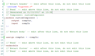
// Component: customComponent
`ifdef CY_BLK_DIR
`undef CY_BLK_DIR
`endif
`ifdef WARP
`define CY_BLK_DIR "C:\Users\xxxx\Documents\Creator\verilogModules\customVerilog.cydsn\customComponent"
`include "C:\Users\xxxx\Documents\Creator\verilogModules\customVerilog.cydsn\customComponent\customComponent.v"
`else
`define CY_BLK_DIR "C:\Users\xxxx\Documents\Creator\verilogModules\customVerilog.cydsn\customComponent"
`include "C:\Users\xxxx\Documents\Creator\verilogModules\customVerilog.cydsn\customComponent\customComponent.v"
`endif
// top
module top ;
wire Net_5;
wire Net_4;
customComponent custom (
.compIn(Net_4),
.compOut(Net_5));
wire [0:0] tmpOE__Pin_1_net;
wire [0:0] tmpFB_0__Pin_1_net;
wire [0:0] tmpIO_0__Pin_1_net;
wire [0:0] tmpINTERRUPT_0__Pin_1_net;
electrical [0:0] tmpSIOVREF__Pin_1_net;
cy_psoc3_pins_v1_10
#(.id("e851a3b9-efb8-48be-bbb8-b303b216c393"),
.drive_mode(3'b110),
.ibuf_enabled(1'b1),
.init_dr_st(1'b0),
.input_clk_en(0),
.input_sync(1'b1),
.input_sync_mode(1'b0),
.intr_mode(2'b00),
.invert_in_clock(0),
.invert_in_clock_en(0),
.invert_in_reset(0),
.invert_out_clock(0),
.invert_out_clock_en(0),
.invert_out_reset(0),
.io_voltage(""),
.layout_mode("CONTIGUOUS"),
.oe_conn(1'b0),
.oe_reset(0),
.oe_sync(1'b0),
.output_clk_en(0),
.output_clock_mode(1'b0),
.output_conn(1'b1),
.output_mode(1'b0),
.output_reset(0),
.output_sync(1'b0),
.pa_in_clock(-1),
.pa_in_clock_en(-1),
.pa_in_reset(-1),
.pa_out_clock(-1),
.pa_out_clock_en(-1),
.pa_out_reset(-1),
.pin_aliases(""),
.pin_mode("O"),
.por_state(4),
.sio_group_cnt(0),
.sio_hyst(1'b1),
.sio_ibuf(""),
.sio_info(2'b00),
.sio_obuf(""),
.sio_refsel(""),
.sio_vtrip(""),
.sio_hifreq(""),
.sio_vohsel(""),
.slew_rate(1'b0),
.spanning(0),
.use_annotation(1'b0),
.vtrip(2'b10),
.width(1),
.ovt_hyst_trim(1'b0),
.ovt_needed(1'b0),
.ovt_slew_control(2'b00),
.input_buffer_sel(2'b00))
Pin_1
(.oe(tmpOE__Pin_1_net),
.y({Net_5}),
.fb({tmpFB_0__Pin_1_net[0:0]}),
.io({tmpIO_0__Pin_1_net[0:0]}),
.siovref(tmpSIOVREF__Pin_1_net),
.interrupt({tmpINTERRUPT_0__Pin_1_net[0:0]}),
.in_clock({1'b0}),
.in_clock_en({1'b1}),
.in_reset({1'b0}),
.out_clock({1'b0}),
.out_clock_en({1'b1}),
.out_reset({1'b0}));
assign tmpOE__Pin_1_net = (`CYDEV_CHIP_MEMBER_USED == `CYDEV_CHIP_MEMBER_3A && `CYDEV_CHIP_REVISION_USED < `CYDEV_CHIP_REVISION_3A_ES3) ? ~{1'b1} : {1'b1};
wire [0:0] tmpOE__Pin_2_net;
wire [0:0] tmpIO_0__Pin_2_net;
wire [0:0] tmpINTERRUPT_0__Pin_2_net;
electrical [0:0] tmpSIOVREF__Pin_2_net;
cy_psoc3_pins_v1_10
#(.id("8d318d8b-cf7b-4b6b-b02c-ab1c5c49d0ba"),
.drive_mode(3'b001),
.ibuf_enabled(1'b1),
.init_dr_st(1'b0),
.input_clk_en(0),
.input_sync(1'b0),
.input_sync_mode(1'b0),
.intr_mode(2'b00),
.invert_in_clock(0),
.invert_in_clock_en(0),
.invert_in_reset(0),
.invert_out_clock(0),
.invert_out_clock_en(0),
.invert_out_reset(0),
.io_voltage(""),
.layout_mode("CONTIGUOUS"),
.oe_conn(1'b0),
.oe_reset(0),
.oe_sync(1'b0),
.output_clk_en(0),
.output_clock_mode(1'b0),
.output_conn(1'b0),
.output_mode(1'b0),
.output_reset(0),
.output_sync(1'b0),
.pa_in_clock(-1),
.pa_in_clock_en(-1),
.pa_in_reset(-1),
.pa_out_clock(-1),
.pa_out_clock_en(-1),
.pa_out_reset(-1),
.pin_aliases(""),
.pin_mode("I"),
.por_state(4),
.sio_group_cnt(0),
.sio_hyst(1'b1),
.sio_ibuf(""),
.sio_info(2'b00),
.sio_obuf(""),
.sio_refsel(""),
.sio_vtrip(""),
.sio_hifreq(""),
.sio_vohsel(""),
.slew_rate(1'b0),
.spanning(0),
.use_annotation(1'b0),
.vtrip(2'b00),
.width(1),
.ovt_hyst_trim(1'b0),
.ovt_needed(1'b0),
.ovt_slew_control(2'b00),
.input_buffer_sel(2'b00))
Pin_2
(.oe(tmpOE__Pin_2_net),
.y({1'b0}),
.fb({Net_4}),
.io({tmpIO_0__Pin_2_net[0:0]}),
.siovref(tmpSIOVREF__Pin_2_net),
.interrupt({tmpINTERRUPT_0__Pin_2_net[0:0]}),
.in_clock({1'b0}),
.in_clock_en({1'b1}),
.in_reset({1'b0}),
.out_clock({1'b0}),
.out_clock_en({1'b1}),
.out_reset({1'b0}));
assign tmpOE__Pin_2_net = (`CYDEV_CHIP_MEMBER_USED == `CYDEV_CHIP_MEMBER_3A && `CYDEV_CHIP_REVISION_USED < `CYDEV_CHIP_REVISION_3A_ES3) ? ~{1'b1} : {1'b1};
endmodule
Here's the verilog from a empty project using the CY8CKIT-059 PSoC 5LP kit:
// ======================================================================
// Design01.v generated from TopDesign.cysch
// 01/11/2017 at 16:34
// This file is auto generated. ANY EDITS YOU MAKE MAY BE LOST WHEN THIS FILE IS REGENERATED!!!
// ======================================================================
/* -- WARNING: The following section of defines are deprecated and will be removed in a future release -- */
`define CYDEV_CHIP_DIE_LEOPARD 1
`define CYDEV_CHIP_REV_LEOPARD_PRODUCTION 3
`define CYDEV_CHIP_REV_LEOPARD_ES3 3
`define CYDEV_CHIP_REV_LEOPARD_ES2 1
`define CYDEV_CHIP_REV_LEOPARD_ES1 0
`define CYDEV_CHIP_DIE_TMA4 2
`define CYDEV_CHIP_REV_TMA4_PRODUCTION 17
`define CYDEV_CHIP_REV_TMA4_ES 17
`define CYDEV_CHIP_REV_TMA4_ES2 33
`define CYDEV_CHIP_DIE_PSOC4A 3
`define CYDEV_CHIP_REV_PSOC4A_PRODUCTION 17
`define CYDEV_CHIP_REV_PSOC4A_ES0 17
`define CYDEV_CHIP_DIE_PSOC5LP 4
`define CYDEV_CHIP_REV_PSOC5LP_PRODUCTION 0
`define CYDEV_CHIP_REV_PSOC5LP_ES0 0
`define CYDEV_CHIP_DIE_PSOC5TM 5
`define CYDEV_CHIP_REV_PSOC5TM_PRODUCTION 1
`define CYDEV_CHIP_REV_PSOC5TM_ES1 1
`define CYDEV_CHIP_REV_PSOC5TM_ES0 0
`define CYDEV_CHIP_DIE_VOLANS 6
`define CYDEV_CHIP_REV_VOLANS_PRODUCTION 0
`define CYDEV_CHIP_DIE_BERRYPECKER 7
`define CYDEV_CHIP_REV_BERRYPECKER_PRODUCTION 0
`define CYDEV_CHIP_DIE_CRANE 8
`define CYDEV_CHIP_REV_CRANE_PRODUCTION 0
`define CYDEV_CHIP_DIE_FM3 9
`define CYDEV_CHIP_REV_FM3_PRODUCTION 0
`define CYDEV_CHIP_DIE_FM4 10
`define CYDEV_CHIP_REV_FM4_PRODUCTION 0
`define CYDEV_CHIP_DIE_EXPECT 4
`define CYDEV_CHIP_REV_EXPECT 0
`define CYDEV_CHIP_DIE_ACTUAL 4
/* -- WARNING: The previous section of defines are deprecated and will be removed in a future release -- */
`define CYDEV_CHIP_FAMILY_PSOC3 1
`define CYDEV_CHIP_FAMILY_PSOC4 2
`define CYDEV_CHIP_FAMILY_PSOC5 3
`define CYDEV_CHIP_FAMILY_FM0P 4
`define CYDEV_CHIP_FAMILY_FM3 5
`define CYDEV_CHIP_FAMILY_FM4 6
`define CYDEV_CHIP_FAMILY_UNKNOWN 0
`define CYDEV_CHIP_MEMBER_UNKNOWN 0
`define CYDEV_CHIP_MEMBER_3A 1
`define CYDEV_CHIP_REVISION_3A_PRODUCTION 3
`define CYDEV_CHIP_REVISION_3A_ES3 3
`define CYDEV_CHIP_REVISION_3A_ES2 1
`define CYDEV_CHIP_REVISION_3A_ES1 0
`define CYDEV_CHIP_MEMBER_4G 2
`define CYDEV_CHIP_REVISION_4G_PRODUCTION 17
`define CYDEV_CHIP_REVISION_4G_ES 17
`define CYDEV_CHIP_REVISION_4G_ES2 33
`define CYDEV_CHIP_MEMBER_4U 3
`define CYDEV_CHIP_REVISION_4U_PRODUCTION 0
`define CYDEV_CHIP_MEMBER_4E 4
`define CYDEV_CHIP_REVISION_4E_PRODUCTION 0
`define CYDEV_CHIP_MEMBER_4O 5
`define CYDEV_CHIP_REVISION_4O_PRODUCTION 0
`define CYDEV_CHIP_MEMBER_4N 6
`define CYDEV_CHIP_REVISION_4N_PRODUCTION 0
`define CYDEV_CHIP_MEMBER_4Q 7
`define CYDEV_CHIP_REVISION_4Q_PRODUCTION 0
`define CYDEV_CHIP_MEMBER_4D 8
`define CYDEV_CHIP_REVISION_4D_PRODUCTION 0
`define CYDEV_CHIP_MEMBER_4J 9
`define CYDEV_CHIP_REVISION_4J_PRODUCTION 0
`define CYDEV_CHIP_MEMBER_4K 10
`define CYDEV_CHIP_REVISION_4K_PRODUCTION 0
`define CYDEV_CHIP_MEMBER_4H 11
`define CYDEV_CHIP_REVISION_4H_PRODUCTION 0
`define CYDEV_CHIP_MEMBER_4A 12
`define CYDEV_CHIP_REVISION_4A_PRODUCTION 17
`define CYDEV_CHIP_REVISION_4A_ES0 17
`define CYDEV_CHIP_MEMBER_4F 13
`define CYDEV_CHIP_REVISION_4F_PRODUCTION 0
`define CYDEV_CHIP_REVISION_4F_PRODUCTION_256K 0
`define CYDEV_CHIP_REVISION_4F_PRODUCTION_256DMA 0
`define CYDEV_CHIP_MEMBER_4P 14
`define CYDEV_CHIP_REVISION_4P_PRODUCTION 0
`define CYDEV_CHIP_MEMBER_4M 15
`define CYDEV_CHIP_REVISION_4M_PRODUCTION 0
`define CYDEV_CHIP_MEMBER_4L 16
`define CYDEV_CHIP_REVISION_4L_PRODUCTION 0
`define CYDEV_CHIP_MEMBER_4I 17
`define CYDEV_CHIP_REVISION_4I_PRODUCTION 0
`define CYDEV_CHIP_MEMBER_4C 18
`define CYDEV_CHIP_REVISION_4C_PRODUCTION 0
`define CYDEV_CHIP_MEMBER_5B 19
`define CYDEV_CHIP_REVISION_5B_PRODUCTION 0
`define CYDEV_CHIP_REVISION_5B_ES0 0
`define CYDEV_CHIP_MEMBER_5A 20
`define CYDEV_CHIP_REVISION_5A_PRODUCTION 1
`define CYDEV_CHIP_REVISION_5A_ES1 1
`define CYDEV_CHIP_REVISION_5A_ES0 0
`define CYDEV_CHIP_MEMBER_PDL_FM0P_TYPE1 21
`define CYDEV_CHIP_REVISION_PDL_FM0P_TYPE1_PRODUCTION 0
`define CYDEV_CHIP_MEMBER_PDL_FM0P_TYPE2 22
`define CYDEV_CHIP_REVISION_PDL_FM0P_TYPE2_PRODUCTION 0
`define CYDEV_CHIP_MEMBER_PDL_FM0P_TYPE3 23
`define CYDEV_CHIP_REVISION_PDL_FM0P_TYPE3_PRODUCTION 0
`define CYDEV_CHIP_MEMBER_FM3 24
`define CYDEV_CHIP_REVISION_FM3_PRODUCTION 0
`define CYDEV_CHIP_MEMBER_FM4 25
`define CYDEV_CHIP_REVISION_FM4_PRODUCTION 0
`define CYDEV_CHIP_FAMILY_USED 3
`define CYDEV_CHIP_MEMBER_USED 19
`define CYDEV_CHIP_REVISION_USED 0
// top
module top ;
endmodule
Digital Output Pin (PSoC 5LP)


That Digital Output Pin with name LED generates:
wire [0:0] tmpOE__LED_net;
wire [0:0] tmpFB_0__LED_net;
wire [0:0] tmpIO_0__LED_net;
wire [0:0] tmpINTERRUPT_0__LED_net;
electrical [0:0] tmpSIOVREF__LED_net;
cy_psoc3_pins_v1_10
#(.id("e851a3b9-efb8-48be-bbb8-b303b216c393"),
.drive_mode(3'b110),
.ibuf_enabled(1'b1),
.init_dr_st(1'b0),
.input_clk_en(0),
.input_sync(1'b1),
.input_sync_mode(1'b0),
.intr_mode(2'b00),
.invert_in_clock(0),
.invert_in_clock_en(0),
.invert_in_reset(0),
.invert_out_clock(0),
.invert_out_clock_en(0),
.invert_out_reset(0),
.io_voltage(""),
.layout_mode("CONTIGUOUS"),
.oe_conn(1'b0),
.oe_reset(0),
.oe_sync(1'b0),
.output_clk_en(0),
.output_clock_mode(1'b0),
.output_conn(1'b0),
.output_mode(1'b0),
.output_reset(0),
.output_sync(1'b0),
.pa_in_clock(-1),
.pa_in_clock_en(-1),
.pa_in_reset(-1),
.pa_out_clock(-1),
.pa_out_clock_en(-1),
.pa_out_reset(-1),
.pin_aliases(""),
.pin_mode("O"),
.por_state(4),
.sio_group_cnt(0),
.sio_hyst(1'b1),
.sio_ibuf(""),
.sio_info(2'b00),
.sio_obuf(""),
.sio_refsel(""),
.sio_vtrip(""),
.sio_hifreq(""),
.sio_vohsel(""),
.slew_rate(1'b0),
.spanning(0),
.use_annotation(1'b0),
.vtrip(2'b10),
.width(1),
.ovt_hyst_trim(1'b0),
.ovt_needed(1'b0),
.ovt_slew_control(2'b00),
.input_buffer_sel(2'b00))
LED
(.oe(tmpOE__LED_net),
.y({1'b0}),
.fb({tmpFB_0__LED_net[0:0]}),
.io({tmpIO_0__LED_net[0:0]}),
.siovref(tmpSIOVREF__LED_net),
.interrupt({tmpINTERRUPT_0__LED_net[0:0]}),
.in_clock({1'b0}),
.in_clock_en({1'b1}),
.in_reset({1'b0}),
.out_clock({1'b0}),
.out_clock_en({1'b1}),
.out_reset({1'b0}));
assign tmpOE__LED_net = (`CYDEV_CHIP_MEMBER_USED == `CYDEV_CHIP_MEMBER_3A && `CYDEV_CHIP_REVISION_USED < `CYDEV_CHIP_REVISION_3A_ES3) ? ~{1'b1} : {1'b1};
Control Register + Digital Output Pin
Here's the design:

// Component: CyControlReg_v1_80
`ifdef CY_BLK_DIR
`undef CY_BLK_DIR
`endif
`ifdef WARP
`define CY_BLK_DIR "C:\Program Files (x86)\Cypress\PSoC Creator\4.0\PSoC Creator\psoc\content\cyprimitives\CyPrimitives.cylib\CyControlReg_v1_80"
`include "C:\Program Files (x86)\Cypress\PSoC Creator\4.0\PSoC Creator\psoc\content\cyprimitives\CyPrimitives.cylib\CyControlReg_v1_80\CyControlReg_v1_80.v"
`else
`define CY_BLK_DIR "C:\Program Files (x86)\Cypress\PSoC Creator\4.0\PSoC Creator\psoc\content\cyprimitives\CyPrimitives.cylib\CyControlReg_v1_80"
`include "C:\Program Files (x86)\Cypress\PSoC Creator\4.0\PSoC Creator\psoc\content\cyprimitives\CyPrimitives.cylib\CyControlReg_v1_80\CyControlReg_v1_80.v"
`endif
// top
module top ;
wire Net_10;
wire Net_9;
wire Net_8;
wire Net_7;
wire Net_6;
wire Net_5;
wire Net_4;
wire Net_3;
wire Net_2;
wire Net_1;
wire [0:0] tmpOE__LED_net;
wire [0:0] tmpFB_0__LED_net;
wire [0:0] tmpIO_0__LED_net;
wire [0:0] tmpINTERRUPT_0__LED_net;
electrical [0:0] tmpSIOVREF__LED_net;
cy_psoc3_pins_v1_10
#(.id("e851a3b9-efb8-48be-bbb8-b303b216c393"),
.drive_mode(3'b110),
.ibuf_enabled(1'b1),
.init_dr_st(1'b0),
.input_clk_en(0),
.input_sync(1'b1),
.input_sync_mode(1'b0),
.intr_mode(2'b00),
.invert_in_clock(0),
.invert_in_clock_en(0),
.invert_in_reset(0),
.invert_out_clock(0),
.invert_out_clock_en(0),
.invert_out_reset(0),
.io_voltage(""),
.layout_mode("CONTIGUOUS"),
.oe_conn(1'b0),
.oe_reset(0),
.oe_sync(1'b0),
.output_clk_en(0),
.output_clock_mode(1'b0),
.output_conn(1'b1),
.output_mode(1'b0),
.output_reset(0),
.output_sync(1'b0),
.pa_in_clock(-1),
.pa_in_clock_en(-1),
.pa_in_reset(-1),
.pa_out_clock(-1),
.pa_out_clock_en(-1),
.pa_out_reset(-1),
.pin_aliases(""),
.pin_mode("O"),
.por_state(4),
.sio_group_cnt(0),
.sio_hyst(1'b1),
.sio_ibuf(""),
.sio_info(2'b00),
.sio_obuf(""),
.sio_refsel(""),
.sio_vtrip(""),
.sio_hifreq(""),
.sio_vohsel(""),
.slew_rate(1'b0),
.spanning(0),
.use_annotation(1'b0),
.vtrip(2'b10),
.width(1),
.ovt_hyst_trim(1'b0),
.ovt_needed(1'b0),
.ovt_slew_control(2'b00),
.input_buffer_sel(2'b00))
LED
(.oe(tmpOE__LED_net),
.y({Net_1}),
.fb({tmpFB_0__LED_net[0:0]}),
.io({tmpIO_0__LED_net[0:0]}),
.siovref(tmpSIOVREF__LED_net),
.interrupt({tmpINTERRUPT_0__LED_net[0:0]}),
.in_clock({1'b0}),
.in_clock_en({1'b1}),
.in_reset({1'b0}),
.out_clock({1'b0}),
.out_clock_en({1'b1}),
.out_reset({1'b0}));
assign tmpOE__LED_net = (`CYDEV_CHIP_MEMBER_USED == `CYDEV_CHIP_MEMBER_3A && `CYDEV_CHIP_REVISION_USED < `CYDEV_CHIP_REVISION_3A_ES3) ? ~{1'b1} : {1'b1};
CyControlReg_v1_80 Control_Reg (
.control_1(Net_2),
.control_2(Net_3),
.control_3(Net_4),
.control_0(Net_1),
.control_4(Net_5),
.control_5(Net_6),
.control_6(Net_7),
.control_7(Net_8),
.clock(1'b0),
.reset(1'b0));
defparam Control_Reg.Bit0Mode = 0;
defparam Control_Reg.Bit1Mode = 0;
defparam Control_Reg.Bit2Mode = 0;
defparam Control_Reg.Bit3Mode = 0;
defparam Control_Reg.Bit4Mode = 0;
defparam Control_Reg.Bit5Mode = 0;
defparam Control_Reg.Bit6Mode = 0;
defparam Control_Reg.Bit7Mode = 0;
defparam Control_Reg.BitValue = 0;
defparam Control_Reg.BusDisplay = 0;
defparam Control_Reg.ExtrReset = 0;
defparam Control_Reg.NumOutputs = 1;
endmodule
Control register + Status Register + Clock
This project was done on the 049-42xx kit (PSoC4200 device). I assume the Control and Status verilog modules are the same as on the PSoC5LP, and some `define values changed because of the device family.
// ======================================================================
// PSoC4_Ctrl_Sts.v generated from TopDesign.cysch
// 01/14/2017 at 20:15
// This file is auto generated. ANY EDITS YOU MAKE MAY BE LOST WHEN THIS FILE IS REGENERATED!!!
// ======================================================================
`define CYDEV_CHIP_FAMILY_PSOC3 1
`define CYDEV_CHIP_FAMILY_PSOC4 2
`define CYDEV_CHIP_FAMILY_PSOC5 3
`define CYDEV_CHIP_FAMILY_FM0P 4
`define CYDEV_CHIP_FAMILY_FM3 5
`define CYDEV_CHIP_FAMILY_FM4 6
`define CYDEV_CHIP_FAMILY_UNKNOWN 0
`define CYDEV_CHIP_MEMBER_UNKNOWN 0
`define CYDEV_CHIP_MEMBER_3A 1
`define CYDEV_CHIP_REVISION_3A_PRODUCTION 3
`define CYDEV_CHIP_REVISION_3A_ES3 3
`define CYDEV_CHIP_REVISION_3A_ES2 1
`define CYDEV_CHIP_REVISION_3A_ES1 0
`define CYDEV_CHIP_MEMBER_4G 2
`define CYDEV_CHIP_REVISION_4G_PRODUCTION 17
`define CYDEV_CHIP_REVISION_4G_ES 17
`define CYDEV_CHIP_REVISION_4G_ES2 33
`define CYDEV_CHIP_MEMBER_4U 3
`define CYDEV_CHIP_REVISION_4U_PRODUCTION 0
`define CYDEV_CHIP_MEMBER_4E 4
`define CYDEV_CHIP_REVISION_4E_PRODUCTION 0
`define CYDEV_CHIP_MEMBER_4O 5
`define CYDEV_CHIP_REVISION_4O_PRODUCTION 0
`define CYDEV_CHIP_MEMBER_4N 6
`define CYDEV_CHIP_REVISION_4N_PRODUCTION 0
`define CYDEV_CHIP_MEMBER_4Q 7
`define CYDEV_CHIP_REVISION_4Q_PRODUCTION 0
`define CYDEV_CHIP_MEMBER_4D 8
`define CYDEV_CHIP_REVISION_4D_PRODUCTION 0
`define CYDEV_CHIP_MEMBER_4J 9
`define CYDEV_CHIP_REVISION_4J_PRODUCTION 0
`define CYDEV_CHIP_MEMBER_4K 10
`define CYDEV_CHIP_REVISION_4K_PRODUCTION 0
`define CYDEV_CHIP_MEMBER_4H 11
`define CYDEV_CHIP_REVISION_4H_PRODUCTION 0
`define CYDEV_CHIP_MEMBER_4A 12
`define CYDEV_CHIP_REVISION_4A_PRODUCTION 17
`define CYDEV_CHIP_REVISION_4A_ES0 17
`define CYDEV_CHIP_MEMBER_4F 13
`define CYDEV_CHIP_REVISION_4F_PRODUCTION 0
`define CYDEV_CHIP_REVISION_4F_PRODUCTION_256K 0
`define CYDEV_CHIP_REVISION_4F_PRODUCTION_256DMA 0
`define CYDEV_CHIP_MEMBER_4P 14
`define CYDEV_CHIP_REVISION_4P_PRODUCTION 0
`define CYDEV_CHIP_MEMBER_4M 15
`define CYDEV_CHIP_REVISION_4M_PRODUCTION 0
`define CYDEV_CHIP_MEMBER_4L 16
`define CYDEV_CHIP_REVISION_4L_PRODUCTION 0
`define CYDEV_CHIP_MEMBER_4I 17
`define CYDEV_CHIP_REVISION_4I_PRODUCTION 0
`define CYDEV_CHIP_MEMBER_4C 18
`define CYDEV_CHIP_REVISION_4C_PRODUCTION 0
`define CYDEV_CHIP_MEMBER_5B 19
`define CYDEV_CHIP_REVISION_5B_PRODUCTION 0
`define CYDEV_CHIP_REVISION_5B_ES0 0
`define CYDEV_CHIP_MEMBER_5A 20
`define CYDEV_CHIP_REVISION_5A_PRODUCTION 1
`define CYDEV_CHIP_REVISION_5A_ES1 1
`define CYDEV_CHIP_REVISION_5A_ES0 0
`define CYDEV_CHIP_MEMBER_PDL_FM0P_TYPE1 21
`define CYDEV_CHIP_REVISION_PDL_FM0P_TYPE1_PRODUCTION 0
`define CYDEV_CHIP_MEMBER_PDL_FM0P_TYPE2 22
`define CYDEV_CHIP_REVISION_PDL_FM0P_TYPE2_PRODUCTION 0
`define CYDEV_CHIP_MEMBER_PDL_FM0P_TYPE3 23
`define CYDEV_CHIP_REVISION_PDL_FM0P_TYPE3_PRODUCTION 0
`define CYDEV_CHIP_MEMBER_FM3 24
`define CYDEV_CHIP_REVISION_FM3_PRODUCTION 0
`define CYDEV_CHIP_MEMBER_FM4 25
`define CYDEV_CHIP_REVISION_FM4_PRODUCTION 0
`define CYDEV_CHIP_FAMILY_USED 2
`define CYDEV_CHIP_MEMBER_USED 12
`define CYDEV_CHIP_REVISION_USED 17
// Component: CyControlReg_v1_80
`ifdef CY_BLK_DIR
`undef CY_BLK_DIR
`endif
`ifdef WARP
`define CY_BLK_DIR "C:\Program Files (x86)\Cypress\PSoC Creator\4.0\PSoC Creator\psoc\content\cyprimitives\CyPrimitives.cylib\CyControlReg_v1_80"
`include "C:\Program Files (x86)\Cypress\PSoC Creator\4.0\PSoC Creator\psoc\content\cyprimitives\CyPrimitives.cylib\CyControlReg_v1_80\CyControlReg_v1_80.v"
`else
`define CY_BLK_DIR "C:\Program Files (x86)\Cypress\PSoC Creator\4.0\PSoC Creator\psoc\content\cyprimitives\CyPrimitives.cylib\CyControlReg_v1_80"
`include "C:\Program Files (x86)\Cypress\PSoC Creator\4.0\PSoC Creator\psoc\content\cyprimitives\CyPrimitives.cylib\CyControlReg_v1_80\CyControlReg_v1_80.v"
`endif
// Component: CyStatusReg_v1_90
`ifdef CY_BLK_DIR
`undef CY_BLK_DIR
`endif
`ifdef WARP
`define CY_BLK_DIR "C:\Program Files (x86)\Cypress\PSoC Creator\4.0\PSoC Creator\psoc\content\cyprimitives\CyPrimitives.cylib\CyStatusReg_v1_90"
`include "C:\Program Files (x86)\Cypress\PSoC Creator\4.0\PSoC Creator\psoc\content\cyprimitives\CyPrimitives.cylib\CyStatusReg_v1_90\CyStatusReg_v1_90.v"
`else
`define CY_BLK_DIR "C:\Program Files (x86)\Cypress\PSoC Creator\4.0\PSoC Creator\psoc\content\cyprimitives\CyPrimitives.cylib\CyStatusReg_v1_90"
`include "C:\Program Files (x86)\Cypress\PSoC Creator\4.0\PSoC Creator\psoc\content\cyprimitives\CyPrimitives.cylib\CyStatusReg_v1_90\CyStatusReg_v1_90.v"
`endif
// top
module top ;
wire Net_17;
wire [7:0] Net_13;
wire Net_12;
wire Net_10;
wire Net_9;
wire Net_11;
wire Net_8;
wire Net_7;
wire Net_6;
wire Net_5;
wire Net_3;
wire Net_2;
wire Net_1;
wire Net_4;
CyControlReg_v1_80 Control (
.control_1(Net_1),
.control_2(Net_2),
.control_3(Net_3),
.control_0(Net_4),
.control_4(Net_5),
.control_5(Net_6),
.control_6(Net_7),
.control_7(Net_8),
.clock(1'b0),
.reset(1'b0));
defparam Control.Bit0Mode = 0;
defparam Control.Bit1Mode = 0;
defparam Control.Bit2Mode = 0;
defparam Control.Bit3Mode = 0;
defparam Control.Bit4Mode = 0;
defparam Control.Bit5Mode = 0;
defparam Control.Bit6Mode = 0;
defparam Control.Bit7Mode = 0;
defparam Control.BitValue = 0;
defparam Control.BusDisplay = 0;
defparam Control.ExtrReset = 0;
defparam Control.NumOutputs = 8;
CyStatusReg_v1_90 Status (
.status_0(Net_4),
.status_1(Net_1),
.status_2(Net_2),
.status_3(Net_3),
.clock(Net_11),
.status_4(Net_5),
.status_5(Net_6),
.status_6(Net_7),
.status_7(Net_8),
.intr(Net_12),
.status_bus(8'b0));
defparam Status.Bit0Mode = 0;
defparam Status.Bit1Mode = 0;
defparam Status.Bit2Mode = 0;
defparam Status.Bit3Mode = 0;
defparam Status.Bit4Mode = 0;
defparam Status.Bit5Mode = 0;
defparam Status.Bit6Mode = 0;
defparam Status.Bit7Mode = 0;
defparam Status.BusDisplay = 0;
defparam Status.Interrupt = 0;
defparam Status.MaskValue = 0;
defparam Status.NumInputs = 8;
cy_clock_v1_0
#(.id("774c7934-bd75-45fc-a2b1-92f57c499c45"),
.source_clock_id(""),
.divisor(0),
.period("83333333.3333333"),
.is_direct(0),
.is_digital(0))
clk
(.clock_out(Net_11));
endmodule
XOR Gate
This is done on PSoC5LP device:
Resulting verilog:
// ======================================================================
// XOR.v generated from TopDesign.cysch
// 01/15/2017 at 13:03
// This file is auto generated. ANY EDITS YOU MAKE MAY BE LOST WHEN THIS FILE IS REGENERATED!!!
// ======================================================================
`define CYDEV_CHIP_FAMILY_PSOC3 1
`define CYDEV_CHIP_FAMILY_PSOC4 2
`define CYDEV_CHIP_FAMILY_PSOC5 3
`define CYDEV_CHIP_FAMILY_FM0P 4
`define CYDEV_CHIP_FAMILY_FM3 5
`define CYDEV_CHIP_FAMILY_FM4 6
`define CYDEV_CHIP_FAMILY_UNKNOWN 0
`define CYDEV_CHIP_MEMBER_UNKNOWN 0
`define CYDEV_CHIP_MEMBER_3A 1
`define CYDEV_CHIP_REVISION_3A_PRODUCTION 3
`define CYDEV_CHIP_REVISION_3A_ES3 3
`define CYDEV_CHIP_REVISION_3A_ES2 1
`define CYDEV_CHIP_REVISION_3A_ES1 0
`define CYDEV_CHIP_MEMBER_4G 2
`define CYDEV_CHIP_REVISION_4G_PRODUCTION 17
`define CYDEV_CHIP_REVISION_4G_ES 17
`define CYDEV_CHIP_REVISION_4G_ES2 33
`define CYDEV_CHIP_MEMBER_4U 3
`define CYDEV_CHIP_REVISION_4U_PRODUCTION 0
`define CYDEV_CHIP_MEMBER_4E 4
`define CYDEV_CHIP_REVISION_4E_PRODUCTION 0
`define CYDEV_CHIP_MEMBER_4O 5
`define CYDEV_CHIP_REVISION_4O_PRODUCTION 0
`define CYDEV_CHIP_MEMBER_4N 6
`define CYDEV_CHIP_REVISION_4N_PRODUCTION 0
`define CYDEV_CHIP_MEMBER_4Q 7
`define CYDEV_CHIP_REVISION_4Q_PRODUCTION 0
`define CYDEV_CHIP_MEMBER_4D 8
`define CYDEV_CHIP_REVISION_4D_PRODUCTION 0
`define CYDEV_CHIP_MEMBER_4J 9
`define CYDEV_CHIP_REVISION_4J_PRODUCTION 0
`define CYDEV_CHIP_MEMBER_4K 10
`define CYDEV_CHIP_REVISION_4K_PRODUCTION 0
`define CYDEV_CHIP_MEMBER_4H 11
`define CYDEV_CHIP_REVISION_4H_PRODUCTION 0
`define CYDEV_CHIP_MEMBER_4A 12
`define CYDEV_CHIP_REVISION_4A_PRODUCTION 17
`define CYDEV_CHIP_REVISION_4A_ES0 17
`define CYDEV_CHIP_MEMBER_4F 13
`define CYDEV_CHIP_REVISION_4F_PRODUCTION 0
`define CYDEV_CHIP_REVISION_4F_PRODUCTION_256K 0
`define CYDEV_CHIP_REVISION_4F_PRODUCTION_256DMA 0
`define CYDEV_CHIP_MEMBER_4P 14
`define CYDEV_CHIP_REVISION_4P_PRODUCTION 0
`define CYDEV_CHIP_MEMBER_4M 15
`define CYDEV_CHIP_REVISION_4M_PRODUCTION 0
`define CYDEV_CHIP_MEMBER_4L 16
`define CYDEV_CHIP_REVISION_4L_PRODUCTION 0
`define CYDEV_CHIP_MEMBER_4I 17
`define CYDEV_CHIP_REVISION_4I_PRODUCTION 0
`define CYDEV_CHIP_MEMBER_4C 18
`define CYDEV_CHIP_REVISION_4C_PRODUCTION 0
`define CYDEV_CHIP_MEMBER_5B 19
`define CYDEV_CHIP_REVISION_5B_PRODUCTION 0
`define CYDEV_CHIP_REVISION_5B_ES0 0
`define CYDEV_CHIP_MEMBER_5A 20
`define CYDEV_CHIP_REVISION_5A_PRODUCTION 1
`define CYDEV_CHIP_REVISION_5A_ES1 1
`define CYDEV_CHIP_REVISION_5A_ES0 0
`define CYDEV_CHIP_MEMBER_PDL_FM0P_TYPE1 21
`define CYDEV_CHIP_REVISION_PDL_FM0P_TYPE1_PRODUCTION 0
`define CYDEV_CHIP_MEMBER_PDL_FM0P_TYPE2 22
`define CYDEV_CHIP_REVISION_PDL_FM0P_TYPE2_PRODUCTION 0
`define CYDEV_CHIP_MEMBER_PDL_FM0P_TYPE3 23
`define CYDEV_CHIP_REVISION_PDL_FM0P_TYPE3_PRODUCTION 0
`define CYDEV_CHIP_MEMBER_FM3 24
`define CYDEV_CHIP_REVISION_FM3_PRODUCTION 0
`define CYDEV_CHIP_MEMBER_FM4 25
`define CYDEV_CHIP_REVISION_FM4_PRODUCTION 0
`define CYDEV_CHIP_FAMILY_USED 3
`define CYDEV_CHIP_MEMBER_USED 19
`define CYDEV_CHIP_REVISION_USED 0
// Component: xor_v1_0
`ifdef CY_BLK_DIR
`undef CY_BLK_DIR
`endif
`ifdef WARP
`define CY_BLK_DIR "C:\Program Files (x86)\Cypress\PSoC Creator\4.0\PSoC Creator\psoc\content\cyprimitives\CyPrimitives.cylib\xor_v1_0"
`include "C:\Program Files (x86)\Cypress\PSoC Creator\4.0\PSoC Creator\psoc\content\cyprimitives\CyPrimitives.cylib\xor_v1_0\xor_v1_0.v"
`else
`define CY_BLK_DIR "C:\Program Files (x86)\Cypress\PSoC Creator\4.0\PSoC Creator\psoc\content\cyprimitives\CyPrimitives.cylib\xor_v1_0"
`include "C:\Program Files (x86)\Cypress\PSoC Creator\4.0\PSoC Creator\psoc\content\cyprimitives\CyPrimitives.cylib\xor_v1_0\xor_v1_0.v"
`endif
// top
module top ;
wire Net_3;
wire Net_2;
wire Net_1;
assign Net_3 = Net_1 ^ Net_2;
wire [0:0] tmpOE__Pin_1_net;
wire [0:0] tmpFB_0__Pin_1_net;
wire [0:0] tmpIO_0__Pin_1_net;
wire [0:0] tmpINTERRUPT_0__Pin_1_net;
electrical [0:0] tmpSIOVREF__Pin_1_net;
cy_psoc3_pins_v1_10
#(.id("e851a3b9-efb8-48be-bbb8-b303b216c393"),
.drive_mode(3'b110),
.ibuf_enabled(1'b1),
.init_dr_st(1'b0),
.input_clk_en(0),
.input_sync(1'b1),
.input_sync_mode(1'b0),
.intr_mode(2'b00),
.invert_in_clock(0),
.invert_in_clock_en(0),
.invert_in_reset(0),
.invert_out_clock(0),
.invert_out_clock_en(0),
.invert_out_reset(0),
.io_voltage(""),
.layout_mode("CONTIGUOUS"),
.oe_conn(1'b0),
.oe_reset(0),
.oe_sync(1'b0),
.output_clk_en(0),
.output_clock_mode(1'b0),
.output_conn(1'b1),
.output_mode(1'b0),
.output_reset(0),
.output_sync(1'b0),
.pa_in_clock(-1),
.pa_in_clock_en(-1),
.pa_in_reset(-1),
.pa_out_clock(-1),
.pa_out_clock_en(-1),
.pa_out_reset(-1),
.pin_aliases(""),
.pin_mode("O"),
.por_state(4),
.sio_group_cnt(0),
.sio_hyst(1'b1),
.sio_ibuf(""),
.sio_info(2'b00),
.sio_obuf(""),
.sio_refsel(""),
.sio_vtrip(""),
.sio_hifreq(""),
.sio_vohsel(""),
.slew_rate(1'b0),
.spanning(0),
.use_annotation(1'b0),
.vtrip(2'b10),
.width(1),
.ovt_hyst_trim(1'b0),
.ovt_needed(1'b0),
.ovt_slew_control(2'b00),
.input_buffer_sel(2'b00))
Pin_1
(.oe(tmpOE__Pin_1_net),
.y({Net_3}),
.fb({tmpFB_0__Pin_1_net[0:0]}),
.io({tmpIO_0__Pin_1_net[0:0]}),
.siovref(tmpSIOVREF__Pin_1_net),
.interrupt({tmpINTERRUPT_0__Pin_1_net[0:0]}),
.in_clock({1'b0}),
.in_clock_en({1'b1}),
.in_reset({1'b0}),
.out_clock({1'b0}),
.out_clock_en({1'b1}),
.out_reset({1'b0}));
assign tmpOE__Pin_1_net = (`CYDEV_CHIP_MEMBER_USED == `CYDEV_CHIP_MEMBER_3A && `CYDEV_CHIP_REVISION_USED < `CYDEV_CHIP_REVISION_3A_ES3) ? ~{1'b1} : {1'b1};
wire [0:0] tmpOE__Pin_2_net;
wire [0:0] tmpIO_0__Pin_2_net;
wire [0:0] tmpINTERRUPT_0__Pin_2_net;
electrical [0:0] tmpSIOVREF__Pin_2_net;
cy_psoc3_pins_v1_10
#(.id("8d318d8b-cf7b-4b6b-b02c-ab1c5c49d0ba"),
.drive_mode(3'b001),
.ibuf_enabled(1'b1),
.init_dr_st(1'b0),
.input_clk_en(0),
.input_sync(1'b0),
.input_sync_mode(1'b0),
.intr_mode(2'b00),
.invert_in_clock(0),
.invert_in_clock_en(0),
.invert_in_reset(0),
.invert_out_clock(0),
.invert_out_clock_en(0),
.invert_out_reset(0),
.io_voltage(""),
.layout_mode("CONTIGUOUS"),
.oe_conn(1'b0),
.oe_reset(0),
.oe_sync(1'b0),
.output_clk_en(0),
.output_clock_mode(1'b0),
.output_conn(1'b0),
.output_mode(1'b0),
.output_reset(0),
.output_sync(1'b0),
.pa_in_clock(-1),
.pa_in_clock_en(-1),
.pa_in_reset(-1),
.pa_out_clock(-1),
.pa_out_clock_en(-1),
.pa_out_reset(-1),
.pin_aliases(""),
.pin_mode("I"),
.por_state(4),
.sio_group_cnt(0),
.sio_hyst(1'b1),
.sio_ibuf(""),
.sio_info(2'b00),
.sio_obuf(""),
.sio_refsel(""),
.sio_vtrip(""),
.sio_hifreq(""),
.sio_vohsel(""),
.slew_rate(1'b0),
.spanning(0),
.use_annotation(1'b0),
.vtrip(2'b00),
.width(1),
.ovt_hyst_trim(1'b0),
.ovt_needed(1'b0),
.ovt_slew_control(2'b00),
.input_buffer_sel(2'b00))
Pin_2
(.oe(tmpOE__Pin_2_net),
.y({1'b0}),
.fb({Net_1}),
.io({tmpIO_0__Pin_2_net[0:0]}),
.siovref(tmpSIOVREF__Pin_2_net),
.interrupt({tmpINTERRUPT_0__Pin_2_net[0:0]}),
.in_clock({1'b0}),
.in_clock_en({1'b1}),
.in_reset({1'b0}),
.out_clock({1'b0}),
.out_clock_en({1'b1}),
.out_reset({1'b0}));
assign tmpOE__Pin_2_net = (`CYDEV_CHIP_MEMBER_USED == `CYDEV_CHIP_MEMBER_3A && `CYDEV_CHIP_REVISION_USED < `CYDEV_CHIP_REVISION_3A_ES3) ? ~{1'b1} : {1'b1};
wire [0:0] tmpOE__Pin_3_net;
wire [0:0] tmpIO_0__Pin_3_net;
wire [0:0] tmpINTERRUPT_0__Pin_3_net;
electrical [0:0] tmpSIOVREF__Pin_3_net;
cy_psoc3_pins_v1_10
#(.id("bf50db59-6b22-44ef-b1f1-1f090f6cf318"),
.drive_mode(3'b001),
.ibuf_enabled(1'b1),
.init_dr_st(1'b0),
.input_clk_en(0),
.input_sync(1'b0),
.input_sync_mode(1'b0),
.intr_mode(2'b00),
.invert_in_clock(0),
.invert_in_clock_en(0),
.invert_in_reset(0),
.invert_out_clock(0),
.invert_out_clock_en(0),
.invert_out_reset(0),
.io_voltage(""),
.layout_mode("CONTIGUOUS"),
.oe_conn(1'b0),
.oe_reset(0),
.oe_sync(1'b0),
.output_clk_en(0),
.output_clock_mode(1'b0),
.output_conn(1'b0),
.output_mode(1'b0),
.output_reset(0),
.output_sync(1'b0),
.pa_in_clock(-1),
.pa_in_clock_en(-1),
.pa_in_reset(-1),
.pa_out_clock(-1),
.pa_out_clock_en(-1),
.pa_out_reset(-1),
.pin_aliases(""),
.pin_mode("I"),
.por_state(4),
.sio_group_cnt(0),
.sio_hyst(1'b1),
.sio_ibuf(""),
.sio_info(2'b00),
.sio_obuf(""),
.sio_refsel(""),
.sio_vtrip(""),
.sio_hifreq(""),
.sio_vohsel(""),
.slew_rate(1'b0),
.spanning(0),
.use_annotation(1'b0),
.vtrip(2'b00),
.width(1),
.ovt_hyst_trim(1'b0),
.ovt_needed(1'b0),
.ovt_slew_control(2'b00),
.input_buffer_sel(2'b00))
Pin_3
(.oe(tmpOE__Pin_3_net),
.y({1'b0}),
.fb({Net_2}),
.io({tmpIO_0__Pin_3_net[0:0]}),
.siovref(tmpSIOVREF__Pin_3_net),
.interrupt({tmpINTERRUPT_0__Pin_3_net[0:0]}),
.in_clock({1'b0}),
.in_clock_en({1'b1}),
.in_reset({1'b0}),
.out_clock({1'b0}),
.out_clock_en({1'b1}),
.out_reset({1'b0}));
assign tmpOE__Pin_3_net = (`CYDEV_CHIP_MEMBER_USED == `CYDEV_CHIP_MEMBER_3A && `CYDEV_CHIP_REVISION_USED < `CYDEV_CHIP_REVISION_3A_ES3) ? ~{1'b1} : {1'b1};
endmodule
Custom verilog component
This is done on PSoC5LP device, the component verilog is the following:
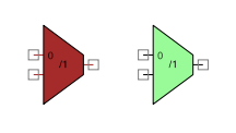
The custom component symbol:

// ======================================================================
// customVerilog.v generated from TopDesign.cysch
// 01/15/2017 at 13:40
// This file is auto generated. ANY EDITS YOU MAKE MAY BE LOST WHEN THIS FILE IS REGENERATED!!!
// ======================================================================
`define CYDEV_CHIP_FAMILY_PSOC3 1
`define CYDEV_CHIP_FAMILY_PSOC4 2
`define CYDEV_CHIP_FAMILY_PSOC5 3
`define CYDEV_CHIP_FAMILY_FM0P 4
`define CYDEV_CHIP_FAMILY_FM3 5
`define CYDEV_CHIP_FAMILY_FM4 6
`define CYDEV_CHIP_FAMILY_UNKNOWN 0
`define CYDEV_CHIP_MEMBER_UNKNOWN 0
`define CYDEV_CHIP_MEMBER_3A 1
`define CYDEV_CHIP_REVISION_3A_PRODUCTION 3
`define CYDEV_CHIP_REVISION_3A_ES3 3
`define CYDEV_CHIP_REVISION_3A_ES2 1
`define CYDEV_CHIP_REVISION_3A_ES1 0
`define CYDEV_CHIP_MEMBER_4G 2
`define CYDEV_CHIP_REVISION_4G_PRODUCTION 17
`define CYDEV_CHIP_REVISION_4G_ES 17
`define CYDEV_CHIP_REVISION_4G_ES2 33
`define CYDEV_CHIP_MEMBER_4U 3
`define CYDEV_CHIP_REVISION_4U_PRODUCTION 0
`define CYDEV_CHIP_MEMBER_4E 4
`define CYDEV_CHIP_REVISION_4E_PRODUCTION 0
`define CYDEV_CHIP_MEMBER_4O 5
`define CYDEV_CHIP_REVISION_4O_PRODUCTION 0
`define CYDEV_CHIP_MEMBER_4N 6
`define CYDEV_CHIP_REVISION_4N_PRODUCTION 0
`define CYDEV_CHIP_MEMBER_4Q 7
`define CYDEV_CHIP_REVISION_4Q_PRODUCTION 0
`define CYDEV_CHIP_MEMBER_4D 8
`define CYDEV_CHIP_REVISION_4D_PRODUCTION 0
`define CYDEV_CHIP_MEMBER_4J 9
`define CYDEV_CHIP_REVISION_4J_PRODUCTION 0
`define CYDEV_CHIP_MEMBER_4K 10
`define CYDEV_CHIP_REVISION_4K_PRODUCTION 0
`define CYDEV_CHIP_MEMBER_4H 11
`define CYDEV_CHIP_REVISION_4H_PRODUCTION 0
`define CYDEV_CHIP_MEMBER_4A 12
`define CYDEV_CHIP_REVISION_4A_PRODUCTION 17
`define CYDEV_CHIP_REVISION_4A_ES0 17
`define CYDEV_CHIP_MEMBER_4F 13
`define CYDEV_CHIP_REVISION_4F_PRODUCTION 0
`define CYDEV_CHIP_REVISION_4F_PRODUCTION_256K 0
`define CYDEV_CHIP_REVISION_4F_PRODUCTION_256DMA 0
`define CYDEV_CHIP_MEMBER_4P 14
`define CYDEV_CHIP_REVISION_4P_PRODUCTION 0
`define CYDEV_CHIP_MEMBER_4M 15
`define CYDEV_CHIP_REVISION_4M_PRODUCTION 0
`define CYDEV_CHIP_MEMBER_4L 16
`define CYDEV_CHIP_REVISION_4L_PRODUCTION 0
`define CYDEV_CHIP_MEMBER_4I 17
`define CYDEV_CHIP_REVISION_4I_PRODUCTION 0
`define CYDEV_CHIP_MEMBER_4C 18
`define CYDEV_CHIP_REVISION_4C_PRODUCTION 0
`define CYDEV_CHIP_MEMBER_5B 19
`define CYDEV_CHIP_REVISION_5B_PRODUCTION 0
`define CYDEV_CHIP_REVISION_5B_ES0 0
`define CYDEV_CHIP_MEMBER_5A 20
`define CYDEV_CHIP_REVISION_5A_PRODUCTION 1
`define CYDEV_CHIP_REVISION_5A_ES1 1
`define CYDEV_CHIP_REVISION_5A_ES0 0
`define CYDEV_CHIP_MEMBER_PDL_FM0P_TYPE1 21
`define CYDEV_CHIP_REVISION_PDL_FM0P_TYPE1_PRODUCTION 0
`define CYDEV_CHIP_MEMBER_PDL_FM0P_TYPE2 22
`define CYDEV_CHIP_REVISION_PDL_FM0P_TYPE2_PRODUCTION 0
`define CYDEV_CHIP_MEMBER_PDL_FM0P_TYPE3 23
`define CYDEV_CHIP_REVISION_PDL_FM0P_TYPE3_PRODUCTION 0
`define CYDEV_CHIP_MEMBER_FM3 24
`define CYDEV_CHIP_REVISION_FM3_PRODUCTION 0
`define CYDEV_CHIP_MEMBER_FM4 25
`define CYDEV_CHIP_REVISION_FM4_PRODUCTION 0
`define CYDEV_CHIP_FAMILY_USED 3
`define CYDEV_CHIP_MEMBER_USED 19
`define CYDEV_CHIP_REVISION_USED 0
// Component: customComponent
`ifdef CY_BLK_DIR
`undef CY_BLK_DIR
`endif
`ifdef WARP
`define CY_BLK_DIR "C:\Users\xxxx\Documents\Creator\verilogModules\customVerilog.cydsn\customComponent"
`include "C:\Users\xxxx\Documents\Creator\verilogModules\customVerilog.cydsn\customComponent\customComponent.v"
`else
`define CY_BLK_DIR "C:\Users\xxxx\Documents\Creator\verilogModules\customVerilog.cydsn\customComponent"
`include "C:\Users\xxxx\Documents\Creator\verilogModules\customVerilog.cydsn\customComponent\customComponent.v"
`endif
// top
module top ;
wire Net_5;
wire Net_4;
customComponent custom (
.compIn(Net_4),
.compOut(Net_5));
wire [0:0] tmpOE__Pin_1_net;
wire [0:0] tmpFB_0__Pin_1_net;
wire [0:0] tmpIO_0__Pin_1_net;
wire [0:0] tmpINTERRUPT_0__Pin_1_net;
electrical [0:0] tmpSIOVREF__Pin_1_net;
cy_psoc3_pins_v1_10
#(.id("e851a3b9-efb8-48be-bbb8-b303b216c393"),
.drive_mode(3'b110),
.ibuf_enabled(1'b1),
.init_dr_st(1'b0),
.input_clk_en(0),
.input_sync(1'b1),
.input_sync_mode(1'b0),
.intr_mode(2'b00),
.invert_in_clock(0),
.invert_in_clock_en(0),
.invert_in_reset(0),
.invert_out_clock(0),
.invert_out_clock_en(0),
.invert_out_reset(0),
.io_voltage(""),
.layout_mode("CONTIGUOUS"),
.oe_conn(1'b0),
.oe_reset(0),
.oe_sync(1'b0),
.output_clk_en(0),
.output_clock_mode(1'b0),
.output_conn(1'b1),
.output_mode(1'b0),
.output_reset(0),
.output_sync(1'b0),
.pa_in_clock(-1),
.pa_in_clock_en(-1),
.pa_in_reset(-1),
.pa_out_clock(-1),
.pa_out_clock_en(-1),
.pa_out_reset(-1),
.pin_aliases(""),
.pin_mode("O"),
.por_state(4),
.sio_group_cnt(0),
.sio_hyst(1'b1),
.sio_ibuf(""),
.sio_info(2'b00),
.sio_obuf(""),
.sio_refsel(""),
.sio_vtrip(""),
.sio_hifreq(""),
.sio_vohsel(""),
.slew_rate(1'b0),
.spanning(0),
.use_annotation(1'b0),
.vtrip(2'b10),
.width(1),
.ovt_hyst_trim(1'b0),
.ovt_needed(1'b0),
.ovt_slew_control(2'b00),
.input_buffer_sel(2'b00))
Pin_1
(.oe(tmpOE__Pin_1_net),
.y({Net_5}),
.fb({tmpFB_0__Pin_1_net[0:0]}),
.io({tmpIO_0__Pin_1_net[0:0]}),
.siovref(tmpSIOVREF__Pin_1_net),
.interrupt({tmpINTERRUPT_0__Pin_1_net[0:0]}),
.in_clock({1'b0}),
.in_clock_en({1'b1}),
.in_reset({1'b0}),
.out_clock({1'b0}),
.out_clock_en({1'b1}),
.out_reset({1'b0}));
assign tmpOE__Pin_1_net = (`CYDEV_CHIP_MEMBER_USED == `CYDEV_CHIP_MEMBER_3A && `CYDEV_CHIP_REVISION_USED < `CYDEV_CHIP_REVISION_3A_ES3) ? ~{1'b1} : {1'b1};
wire [0:0] tmpOE__Pin_2_net;
wire [0:0] tmpIO_0__Pin_2_net;
wire [0:0] tmpINTERRUPT_0__Pin_2_net;
electrical [0:0] tmpSIOVREF__Pin_2_net;
cy_psoc3_pins_v1_10
#(.id("8d318d8b-cf7b-4b6b-b02c-ab1c5c49d0ba"),
.drive_mode(3'b001),
.ibuf_enabled(1'b1),
.init_dr_st(1'b0),
.input_clk_en(0),
.input_sync(1'b0),
.input_sync_mode(1'b0),
.intr_mode(2'b00),
.invert_in_clock(0),
.invert_in_clock_en(0),
.invert_in_reset(0),
.invert_out_clock(0),
.invert_out_clock_en(0),
.invert_out_reset(0),
.io_voltage(""),
.layout_mode("CONTIGUOUS"),
.oe_conn(1'b0),
.oe_reset(0),
.oe_sync(1'b0),
.output_clk_en(0),
.output_clock_mode(1'b0),
.output_conn(1'b0),
.output_mode(1'b0),
.output_reset(0),
.output_sync(1'b0),
.pa_in_clock(-1),
.pa_in_clock_en(-1),
.pa_in_reset(-1),
.pa_out_clock(-1),
.pa_out_clock_en(-1),
.pa_out_reset(-1),
.pin_aliases(""),
.pin_mode("I"),
.por_state(4),
.sio_group_cnt(0),
.sio_hyst(1'b1),
.sio_ibuf(""),
.sio_info(2'b00),
.sio_obuf(""),
.sio_refsel(""),
.sio_vtrip(""),
.sio_hifreq(""),
.sio_vohsel(""),
.slew_rate(1'b0),
.spanning(0),
.use_annotation(1'b0),
.vtrip(2'b00),
.width(1),
.ovt_hyst_trim(1'b0),
.ovt_needed(1'b0),
.ovt_slew_control(2'b00),
.input_buffer_sel(2'b00))
Pin_2
(.oe(tmpOE__Pin_2_net),
.y({1'b0}),
.fb({Net_4}),
.io({tmpIO_0__Pin_2_net[0:0]}),
.siovref(tmpSIOVREF__Pin_2_net),
.interrupt({tmpINTERRUPT_0__Pin_2_net[0:0]}),
.in_clock({1'b0}),
.in_clock_en({1'b1}),
.in_reset({1'b0}),
.out_clock({1'b0}),
.out_clock_en({1'b1}),
.out_reset({1'b0}));
assign tmpOE__Pin_2_net = (`CYDEV_CHIP_MEMBER_USED == `CYDEV_CHIP_MEMBER_3A && `CYDEV_CHIP_REVISION_USED < `CYDEV_CHIP_REVISION_3A_ES3) ? ~{1'b1} : {1'b1};
endmodule

Comentarios
Publicar un comentario